Low-leakage SiC Schottky diode and manufacturing method thereof
A technology of Schottky diode and manufacturing method, which is applied in the manufacturing of circuits, electrical components, semiconductor/solid-state devices, etc., can solve the problems of large reverse blocking consumption, large reverse leakage current, reduced circuit efficiency, etc. The effect of reverse blocking loss, reducing leakage problems, improving reliability and yield
- Summary
- Abstract
- Description
- Claims
- Application Information
AI Technical Summary
Problems solved by technology
Method used
Image

Examples
Embodiment 1
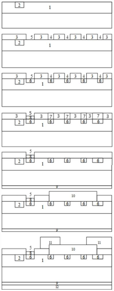
[0043] This embodiment is prepared according to the manufacturing method of the low-leakage SiC Schottky diode provided by the present invention, including the following steps:
[0044] Step 21: Provide an epitaxial chip, the epitaxial chip is on the N+ substrate, a silicon carbide epitaxial layer is formed on the epitaxial chip, and the epitaxial layer is coated with photoresist, and an inductively coupled plasma etching machine is used for the epitaxial layer. layer uses C 4 f 8 and SF 6 Etching is carried out in an alternate etching manner, and the alignment mark is photoetched, C4 f 8 The flow rate during etching is 200sccm, SF 6 The flow rate during etching is 100sccm, the etching time is 60min, and the etching is completed to obtain a plate registration mark with an etching depth of 50nm;
[0045] Step 22, depositing SiO on the surface of the silicon carbide epitaxial layer 2 An oxide layer, wherein the deposited thickness of the oxide layer is 1500nm;
[0046] Ste...
Embodiment 2
[0055] This embodiment is prepared according to the manufacturing method of the low-leakage SiC Schottky diode provided by the present invention, including the following steps:
[0056] Step 31: Provide an epitaxial chip, the epitaxial chip is on the N+ substrate, form a silicon carbide epitaxial layer on the epitaxial chip, coat the epitaxial layer with photoresist, use an inductively coupled plasma etching machine, layer uses C 4 f 8 and SF 6 Etching is carried out in an alternate etching method, and the alignment mark is photoetched, the etching time is 2min, C 4 f 8 The flow rate during etching is 2000sccm, SF 6 The flow rate during etching is 500 sccm, and the etching is completed to obtain a plate registration mark with an etching depth of 1 μm;
[0057] Step 32, depositing SiO on the surface of the silicon carbide epitaxial layer 2 An oxide layer, wherein the deposition thickness of the oxide layer is 3000nm;
[0058] Step 33, performing photolithography on the s...
Embodiment 3
[0067] This embodiment is prepared according to the manufacturing method of the low-leakage SiC Schottky diode provided by the present invention, including the following steps:
[0068] Step 41: Provide an epitaxial chip, the epitaxial chip is on the N+ substrate, form a silicon carbide epitaxial layer on the epitaxial chip, coat the epitaxial layer with photoresist, use an inductively coupled plasma etching machine, layer uses C 4 f 8 and SF 6 Etching is carried out in an alternate etching method, and the alignment mark is photoetched, the etching time is 30min, C 4 f 8 The flow rate during etching is 1000sccm, SF 6 The flow rate during etching is 300sccm, and the etching depth is 500nm to obtain the plate alignment mark;
[0069] Step 42, depositing SiO on the surface of the silicon carbide epitaxial layer 2 An oxide layer, wherein the deposition thickness of the oxide layer is 2000nm;
[0070] Step 43, performing photolithography on the surface of the oxide layer to ...
PUM
| Property | Measurement | Unit |
|---|---|---|
| Deposition thickness | aaaaa | aaaaa |
| Deposition thickness | aaaaa | aaaaa |
| Thickness | aaaaa | aaaaa |
Abstract
Description
Claims
Application Information
 - R&D
- Intellectual Property
- Life Sciences
- Materials
- Tech Scout
- Unparalleled Data Quality
- Higher Quality Content
- 60% Fewer Hallucinations
Browse by: Latest US Patents, China's latest patents, Technical Efficacy Thesaurus, Application Domain, Technology Topic, Popular Technical Reports.
© 2025 PatSnap. All rights reserved.Legal|Privacy policy|Modern Slavery Act Transparency Statement|Sitemap|About US| Contact US: help@patsnap.com