
A kind of preparation method of low stress TIW film

A low-stress, thin-film technology, applied in metal material coating process, vacuum evaporation coating, coating and other directions, can solve the problems of decreased interface bonding strength, poor uniformity, and cracked substrate and film, etc. Availability and generalizability, the effect of increasing film nucleation rate and reducing growth stress

Active Publication Date: 2022-07-12
NANCHANG UNIV +1
View PDF1 Cites 0 Cited by
  • Summary
  • Abstract
  • Description
  • Claims
  • Application Information

AI Technical Summary

Problems solved by technology

However, the research on the control of the stress in the specific growth rate of TiW is relatively rough. Relatively, growing a thin film at an excessively small deposition rate will increase the growth time and increase the cost; The temperature of the sheet will continue to rise, resulting in the deposition of a TiW film with poor uniformity and low density. In addition, for semiconductor devices, an excessive deposition rate will cause excessive internal stress of the metallization film layer, and the internal stress of the TiW film will be too large. The structural layer of the device is deformed and warped until the adhesion of the interface bonding strength decreases, the substrate and the film layer will break and cause the device to fail, and problems such as voltage instability and life shortening will occur.

Method used

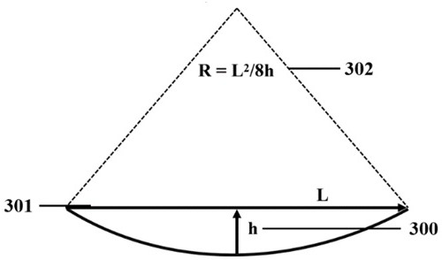

Image

  • A kind of preparation method of low stress TIW film
  • A kind of preparation method of low stress TIW film
  • A kind of preparation method of low stress TIW film

Examples


Embodiment Construction

[0021] The present invention will be described in further detail below with reference to the accompanying drawings and specific examples, but the embodiments of the present invention include but are not limited to the scopes indicated in the following examples.

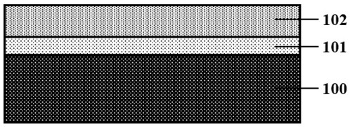
[0022] refer to figure 1 , a schematic diagram of the structure of a low-stress TiW thin film, which sequentially includes a substrate, a TiW seed thin film layer, and a TiW main thin film layer from bottom to top. In order to achieve the above purpose, the present invention provides a method for preparing a two-step PVD sputtering low-stress TiW thin film. The main sputtering parameters include DC / RF power, deposition time, argon flow rate, and chamber vacuum pressure. Using the stable growth rate of PVD sputtering method, the deposition power and time are adjusted to precisely control the two-step TiW thin film.

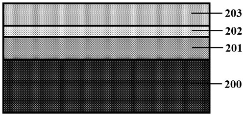
[0023] refer to figure 2 , a schematic diagram of the structure of a two-step PVD sputtering low-str...


PUM

PropertyMeasurementUnit
thicknessaaaaaaaaaa
thicknessaaaaaaaaaa

Abstract

The invention discloses a preparation method of a low-stress TiW film. The method comprises the following steps: growing a thin seed film layer at a small deposition rate and growing a main film layer under a large deposition rate on a substrate of the film to be deposited; by controlling the thickness of the growth and rate, so that the two layers of films can be optimally combined, and a low-stress TiW film can be obtained. In the invention, the TiW film is deposited on the substrate step by step, the seed film layer grown at a small deposition rate has high density, and a highly reliable interface is obtained by mutual fusion with the substrate atoms; the main film layer grown at a large deposition rate is The adhesion of the film grown on the basis of the seed layer buffer is enhanced, so that the thickness of the TiW film is stable and uniform, and the stress on the substrate is weakened and dissipated, so that the deformation amount is small, and the preparation method of the TiW film with low stress and high quality is obtained. The TiW thin film of the present invention can be prepared by common deposition methods, the obtained thin film has high stability, low film layer stress, and has good usability and popularization.

Description

technical field [0001] The invention relates to the field of electronic information semiconductors, in particular to a preparation method of a low-stress TiW thin film. Background technique [0002] TiW (Titanium Tungsten) alloy material is formed by doped tungsten particles in titanium metal. Due to its high strength, wear resistance, good toughness and light weight, TiW alloy is widely used in aerospace devices and components. Manufacturing, medical equipment, light industry and other fields. In addition to the above characteristics, with the rapid development of electronic information and semiconductor ultra-large-scale integrated circuit industries, TiW alloys also have low electron mobility, stable thermomechanical properties, corrosion resistance and their chemical stability. Diffusion barrier layers are used in semiconductor chips, especially in high temperature and high current environments. Through the process of preparing high-purity thin films, they are widely us...

Claims


Application Information

Patent Timeline
Patent Type & Authority Patents(China)
IPC IPC(8): C23C14/16C23C14/18C23C14/22
CPCC23C14/16C23C14/18C23C14/22
Inventor 吴小明王子超陈芳王光绪陶喜霞
Owner NANCHANG UNIV
Learn More