4H-SiC PIN microwave diode based on gradient doping of P region and I region and manufacturing method of 4H-SiC PIN microwave diode

A gradient doping, diode technology, applied in semiconductor/solid-state device manufacturing, electrical components, circuits, etc., can solve problems such as being unsuitable for microwave circuits, and achieve improved power characteristics and reliability, low zero-bias junction capacitance, and low conductance. The effect of on-resistance

Active Publication Date: 2021-10-26
XIDIAN UNIV
View PDF9 Cites 0 Cited by
  • Summary
  • Abstract
  • Description
  • Claims
  • Application Information

AI Technical Summary

Problems solved by technology

However, when the device is used as a radio frequency device, it is not suitable for microwave circuits due to its large I-region width.
At present, 4H-SiC PIN diodes for microwave need smaller on-resistance and lower junction capacitance to meet faster response speed, but the existing 4H-SiC PIN diodes cannot meet the requirements, resulting in their existence in the field of high-frequency microwave applications. big vacancy

Method used


Image

  • 4H-SiC PIN microwave diode based on gradient doping of P region and I region and manufacturing method of 4H-SiC PIN microwave diode
  • 4H-SiC PIN microwave diode based on gradient doping of P region and I region and manufacturing method of 4H-SiC PIN microwave diode

Examples


Embodiment 1

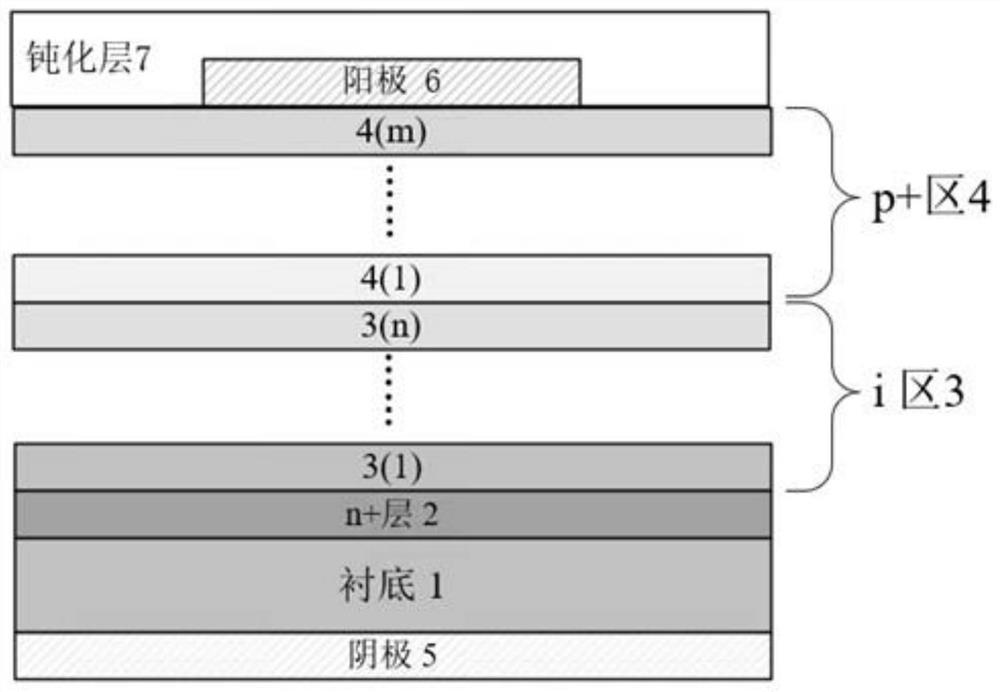
[0034] Example 1, fabricate a graded doped 4H-SiC PIN diode with a single layer thickness of 2 μm in the i region, a layer number n of 2, a single layer thickness of 0.5 μm in the p+ region, and a layer number m of 2.

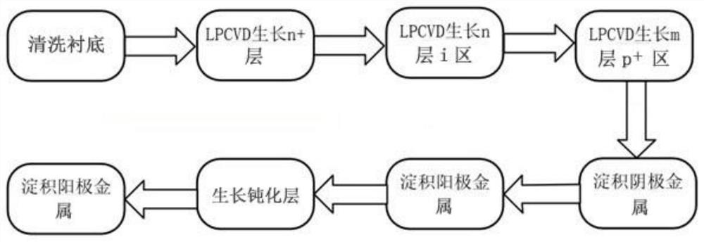
[0035] In step 1, the surface of the 4H-SiC substrate is pretreated to eliminate dangling bonds.

[0036] 1.1) Boil the 4H-SiC substrate in trichlorethylene, acetone, and absolute ethanol for 10-15 min in turn, then wash with deionized water and boil for 10 min, and then in H 2 SO 4 :H 3 PO 3 =Heat 10min in the solution of 3:1, put into deionized water to clean then, to eliminate surface dangling bond;

[0037] 1.2) Use 5% HF solution to remove oxides on the surface of the cleaned substrate.

[0038] Step 2, making n+ layers.

[0039] 2.1) Put the pretreated 4H-SiC substrate into a low-pressure chemical vapor deposition LPCVD system, set the reaction chamber pressure to 10 Torr, and the temperature to 1500°C;

[0040] 2.2) Feed into the reaction chamber s...

Embodiment 2

[0056] Example 2, fabricate a gradiently doped 4H-SiC PIN diode with a single layer thickness of 2 μm in the i region, a layer number n of 3, a single layer thickness of the p+ region of 0.5 μm, and a layer number m of 2.

[0057] In step 1, the surface of the 4H-SiC substrate is pretreated to eliminate dangling bonds.

[0058] The specific implementation of this step is the same as step 1 of Embodiment 1.

[0059] Step 2, making n+ layers.

[0060] Put the pretreated 4H-SiC substrate into the low-pressure chemical vapor deposition LPCVD system, set the reaction chamber pressure to 50Torr, and the temperature to 1500°C; Hydrogen at 1500 sccm, C with a flow rate of 20 sccm 2 h 4 and SiH at a flow rate of 10 sccm 4 , grown on a 4H-SiC substrate with a thickness of 0.5 μm and a doping concentration of 10 19 cm -3 4H-SiC n+ layer.

[0061] Step 3, making multi-layer gradiently doped i-regions.

[0062] A N source with a flow rate of 70 μmol / min, a hydrogen gas with a flow ...

Embodiment 3

[0073] Example 3, fabricate a gradiently doped 4H-SiC PIN diode with a single layer thickness of 2 μm in the i region, a layer number n of 4, a single layer thickness of the p+ region of 0.5 μm, and a layer number m of 3.

[0074] In step A, the surface of the 4H-SiC substrate is pretreated to eliminate dangling bonds.

[0075] The specific implementation of this step is the same as step 1 of Embodiment 1.

[0076] Step B, making n+ layers.

[0077] B1) Put the pretreated 4H-SiC substrate into a low-pressure chemical vapor deposition LPCVD system, set the reaction chamber pressure to 100 Torr, and the temperature to 1500°C;

[0078] B2) Feed into the reaction chamber at the same time a N source with a flow rate of 100 μmol / min, a hydrogen gas with a flow rate of 2500 sccm, and a C source with a flow rate of 16 sccm. 2 h 4 and SiH at a flow rate of 8 sccm 4 , grown on a 4H-SiC substrate with a thickness of 1 μm and a doping concentration of 10 20 cm -3 4H-SiC n+ layer.

...


PUM

PropertyMeasurementUnit
thicknessaaaaaaaaaa
thicknessaaaaaaaaaa
thicknessaaaaaaaaaa

Abstract

The invention discloses a 4H-SiC PIN diode based on gradient doping of a P region and an I region. The 4H-SiC PIN diode mainly solves the problem that low on-resistance and low junction capacitance cannot be achieved in the prior art. The 4H-SiC PIN diode comprises an n-type substrate (1), an n + layer (2), an i layer (3) and a p + layer (4) from bottom to top, a cathode (5) is arranged on the lower portion of the substrate, an anode (6) is arranged on the upper portion of the p + layer, a passivation layer (7) is arranged on the upper portion of the anode, the i layer (3) is of a multi-layer structure composed of n layers, and all the layers are made of 4H-SiC semiconductor materials with linearly decreasing doping concentration; the p + layer (4) is of a multi-layer structure composed of m layers, and each layer is made of a 4H-SiC semiconductor material with linearly increased doping concentration. According to the invention, low on-resistance and low zero bias capacitance can be realized at the same time, the response speed of the PIN diode can be accelerated, the cut-off frequency is improved, and the PIN diode can be used as a microwave diode to be applied to a microwave amplitude limiting circuit.

Description

technical field [0001] The invention belongs to the technical field of semiconductor devices, and in particular relates to a 4H-SiC PIN microwave diode, which can be used in circuits such as microwave rectifiers, amplitude limiters, power switches, phase shifters, and electronically adjustable attenuators. Background technique [0002] PIN diodes are widely used in RF, UHF and microwave circuits. Limiters based on PIN diodes can protect power-sensitive devices in subsequent circuits from being damaged by large signals or strong electromagnetic pulses, so they are widely used in the front-end of transmitting and receiving systems such as communications and radar. By controlling the working state of the PIN diode, when the high-power microwave signal passes through the limiter, it is attenuated to a lower power level, while the low-power microwave signal passes smoothly with a small insertion loss. [0003] Most commercial PIN diodes currently on the market use Si and GaAs. ...

Claims


Application Information

Patent Timeline
Patent Type & Authority Applications(China)
IPC IPC(8): H01L29/16H01L29/06H01L29/868H01L21/329
CPCH01L29/1608H01L29/0611H01L29/868H01L29/6606
Inventor 周弘苏春旭张进成刘志宏许晟瑞郝跃
Owner XIDIAN UNIV
Why Eureka
Try Eureka