Heterojunction tunneling field effect transistor with heterogeneous gate dielectric and manufacturing method thereof

A tunneling field effect and heterogeneous dielectric technology, applied in the field of transistors, can solve the problems of small on-state current and serious bipolar effect, and achieve the effect of increasing the on-state current, suppressing bipolar effect, and increasing the tunneling area

Active Publication Date: 2022-06-03
XIDIAN UNIV
View PDF2 Cites 0 Cited by
  • Summary
  • Abstract
  • Description
  • Claims
  • Application Information

AI Technical Summary

Problems solved by technology

[0004] The purpose of the present invention is to provide a heterojunction tunneling field effect transistor with a heterogeneous gate dielectric and its manufacturing method, so as to solve the problems that the existing silicon-based TFET has the disadvantages of small on-state current and serious bipolar effect

Method used


Image

  • Heterojunction tunneling field effect transistor with heterogeneous gate dielectric and manufacturing method thereof
  • Heterojunction tunneling field effect transistor with heterogeneous gate dielectric and manufacturing method thereof
  • Heterojunction tunneling field effect transistor with heterogeneous gate dielectric and manufacturing method thereof

Examples


Embodiment 1

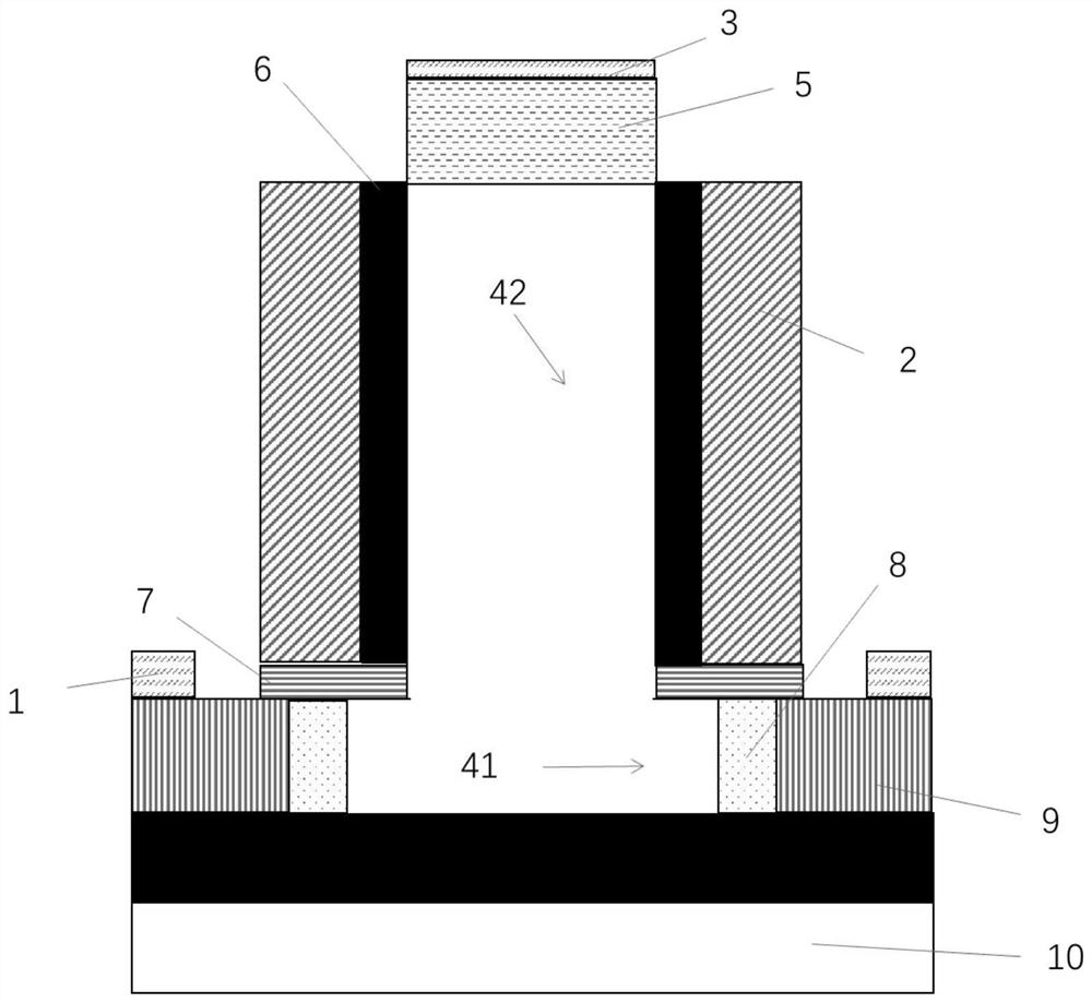
[0033] The present invention provides a heterojunction tunneling field effect transistor of a heterogate dielectric, the tunneling field effect transistor

[0036] Optionally, the material of the first heterogeneous medium 6 is a low-K dielectric material, and / or

[0037] The material of the second heterogeneous medium 7 is a high-K dielectric material.

[0038] Optionally, the first heterogeneous medium 6 is silicon dioxide, and / or the second heterogeneous medium 7 is hafnium oxide.

[0039] Optionally, the tunneling field effect transistor also includes two sides of the source 1 and the "one" portion

[0040] Optionally, the tunneling field effect transistor further includes an SOI substrate 10 under the "a" portion. SOI

[0041] Optionally, the length of the SOI substrate 10 is equal to the length of the "one" part and the length of the "one" part

[0043] N

[0044] P

[0047] N

Embodiment 2

[0050] The present invention also provides a method for making a heterojunction tunneling field effect transistor based on the above-mentioned heterogate dielectric.

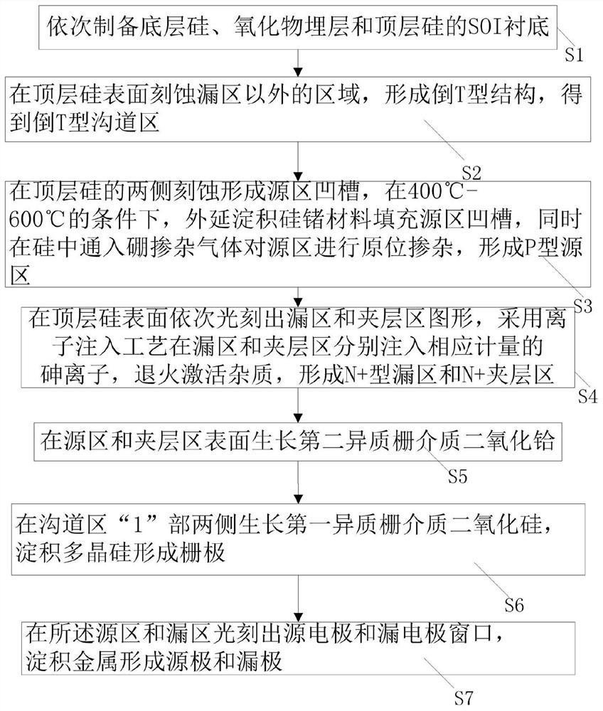
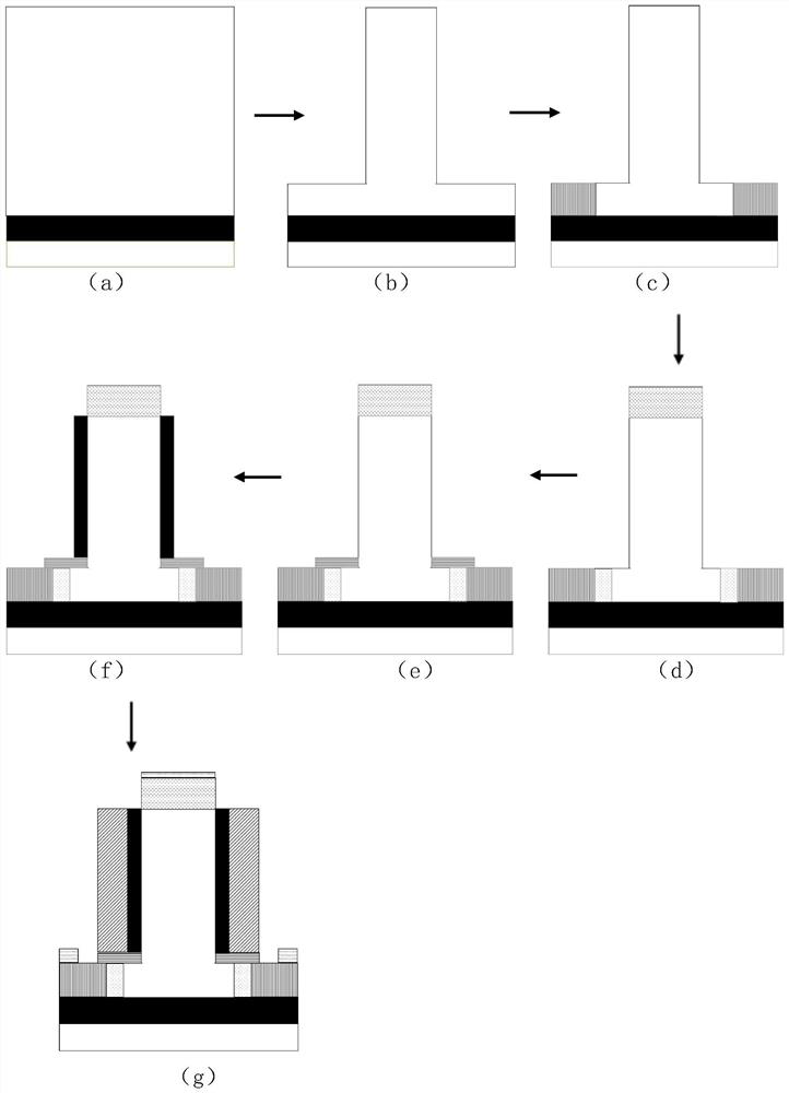
[0052] S1: The SOI substrate 10 of the bottom layer silicon, the oxidized physical layer and the top layer silicon is sequentially prepared.

[0057] S2: Etching the area other than the drain region on the top silicon surface to form an inverted T-type structure to obtain an inverted T-type channel region.

[0058] S21: grow a layer of SiO on the top layer silicon surface

[0064] S33: using a selective epitaxial growth process to deposit a silicon germanium material in the source region groove, and feeding boron doping gas at the same time

[0071] S5: growing a second hetero-gate dielectric hafnium dioxide on the surface of the source region and the interlayer region.

[0075] Step 6: growing a first hetero-gate dielectric 6 silicon dioxide on both sides of the channel region "1", and depositing polysilicon to form...

Embodiment 3

[0086] S12: a silicon epitaxial layer is formed on the surface of the buried oxide layer by epitaxial growth to form an SOI substrate 10;

[0095] S33: using the selective epitaxial growth process to deposit germanium-silicon material in the source region groove, and feeding boron doping gas at the same time

[0097] S4: the preparation doping concentration is 5×10

[0101] Wash off the photoresist, then wash with a hydrofluoric acid HF solution to remove the SiO

[0102] S5: prepare a second hetero-gate dielectric HfO with a thickness of 3 nm

[0106] S6: prepare a first hetero-gate dielectric SiO with a thickness of 3 nm

[0107] S61: using a chemical vapor deposition process at 600° C., the obtained device on both sides of the channel region “1”

[0108] S62: use a dry etching process to etch the gate pattern to form a gate groove; epitaxy in the gate region groove

[0110] S64: use a photoresist mask to protect the gate region and the drain region 5, and selectively etch using ...


PUM

PropertyMeasurementUnit
thicknessaaaaaaaaaa
thicknessaaaaaaaaaa
thicknessaaaaaaaaaa

Abstract

The invention discloses a heterojunction tunneling field effect transistor with a heterogeneous gate dielectric and a manufacturing method thereof, and mainly solves the problems of small on-state current and serious bipolar effect of the existing tunneling field effect transistor. It includes source, gate, drain, source region, channel region and drain region. Carriers enter the channel region through the source and leave the channel region through the drain. The channel region includes "a" part and " 1", the "1" part includes a first connection end connected to the "one" part, and a second connection end opposite to the first connection end, the second connection end is connected to the drain through the drain region, and the "1" part Two gates are arranged on both sides of the two gates, and two first heterogeneous dielectrics are respectively arranged between the two gates and the "1" part, the gates and the first heterogeneous medium are arranged perpendicular to the second heterogeneous medium, and The sum of the heights of the first heterogeneous medium and the second heterogeneous medium is equal to the "1" part, the height of the gate is equal to that of the first heterogeneous medium, and two sources are respectively arranged on both sides of the "1" part.

Description

Heterojunction tunneling field effect transistor with heterogate dielectric and method of making the same technical field The present invention relates to transistor technology field, be specifically related to a kind of heterojunction tunneling field effect crystal of heterogate dielectric Tube and method of making the same. Background technique Thanks to the development of the semiconductor manufacturing process, the feature size of the transistor is continuously reduced, making the integrated circuit to high The direction of performance, low cost continues to develop. However, in traditional CMOS field effect transistors based on thermionic emission mechanism, the low power consumption In the power-consuming digital integrated circuit, since the sub-threshold swing cannot break through the limit of 60mv / dec at room temperature, the power supply voltage cannot follow the device size decreases, resulting in a further increase in the leakage current of the device, a...

Claims


Application Information

Patent Timeline
Patent Type & Authority Patents(China)
IPC IPC(8): H01L29/808H01L21/337H01L29/10
CPCH01L29/808H01L29/66916H01L29/1058
Inventor 段小玲王树龙王刚张进成张涛刘志宏赵胜雷许晟瑞郝跃
Owner XIDIAN UNIV
Why Eureka
Try Eureka