

Resin composition and application thereof
A resin composition and resin technology, applied in the field of laminates, can solve the problems of high tensile strength and peel strength, can not meet the application of thin lines, cannot be obtained, etc., achieve good peel strength, avoid pressure resistance and reliable thin lines Sexual effect, sharp particle size distribution effect
- Summary
- Abstract
- Description
- Claims
- Application Information
AI Technical Summary
Problems solved by technology
Method used
Image

Examples
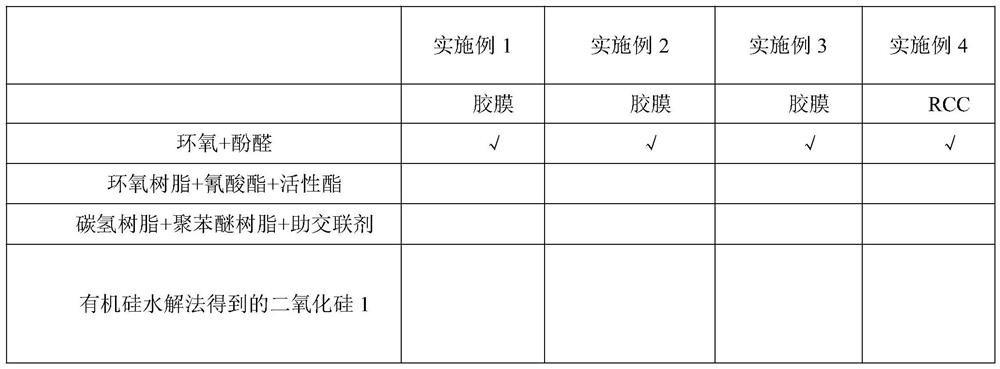
Embodiment 1
[0054] First dissolve 28 parts of epoxy resin (NC-3000H) and 21 parts of phenolic resin (SN-485) with an appropriate amount of solvent, and stir for more than 2 hours.
[0055] Then add 61% of silicon dioxide 3 (D50 is 0.5 μm, D100:D10 is 2.0, and the purity is 99.90%) obtained by organosilicon hydrolysis, and continue to stir for more than 4 hours, and mix well to form a solid content of 70%. solution.
[0056] The above solution was coated on the release film, and after drying, it was put into an oven at 100°C and baked for 5 minutes to obtain an adhesive film of a semi-cured resin layer. Press and cure the semi-cured adhesive film (thickness 40 μm) and the browned PCB board, tear off the release film and then perform surface treatment, copper electroplating, to form a laminated printed circuit board with lines.
Embodiment 2
[0058] Except changing the ratio of silicon dioxide synthesized by the chemical method used in Example 1, the same method as in Example 1 was used to manufacture the adhesive film.
[0059] First dissolve 28 parts of epoxy resin (NC-3000H) and 21 parts of phenolic resin (SN-485) with an appropriate amount of solvent, and stir for more than 2 hours.
[0060] Then add 73% of silicon dioxide 3 (D50 is 0.5 μm, D100:D10 is 2.0, and the purity is 99.90%) obtained by organosilicon hydrolysis, and continue to stir for more than 4 hours, and mix well to form a solid content of 70%. solution.
[0061] Coat the above solution on the release film, dry it, and bake it in an oven at 100°C for 3 minutes to obtain a semi-cured resin layer film. Press and cure the semi-cured adhesive film (thickness 40 μm) and the browned PCB board, tear off the release film and then perform surface treatment, copper electroplating, to form a laminated printed circuit board with lines.
Embodiment 3
[0063] Except changing the ratio of the chemically synthesized silicon dioxide used in Example 1, the same method as in Example 1 was used to manufacture the adhesive film.
[0064] First dissolve 28 parts of epoxy resin (NC-3000H) and 21 parts of phenolic resin (SN-485) with an appropriate amount of solvent, and stir for more than 2 hours.
[0065] Then add 85% silicon dioxide 3 (D50 is 0.5 μm, D100:D10 is 2.0, and the purity is 99.90%) obtained by organosilicon hydrolysis, and continue to stir for more than 4 hours, and mix well to form a solid content of 70%. solution.
[0066] Coat the above solution on the release film, dry it, and bake it in an oven at 100°C for 3 minutes to obtain a semi-cured resin layer film. Press and cure the semi-cured adhesive film (thickness 40 μm) and the browned PCB board, tear off the release film and then perform surface treatment, copper electroplating, to form a laminated printed circuit board with lines.
PUM
| Property | Measurement | Unit |
|---|---|---|
| particle size | aaaaa | aaaaa |
| thickness | aaaaa | aaaaa |
| thickness | aaaaa | aaaaa |
Abstract
Description
Claims
Application Information