Coating carrier and method for increasing TCO coating area of heterojunction solar cell by using same

A solar cell and heterojunction technology, which is applied in the field of solar energy, can solve problems such as mask offset, front-back short-circuit, poor conductivity of amorphous silicon, etc., and achieve the effect of increasing the film-forming area and improving the conversion efficiency

Pending Publication Date: 2021-11-05
晋能光伏技术有限责任公司 +1
View PDF0 Cites 0 Cited by
  • Summary
  • Abstract
  • Description
  • Claims
  • Application Information

AI Technical Summary

Problems solved by technology

[0003] However, the conductivity of amorphous silicon in existing HJT batteries is not good, and it is a common method to cover the surface with a transparent conductive film. At present, there are many types of transparent conductive films including In 2 o 3 , SnO 2 , ZnO, In 2 o 3 :Sn(ITO), In 2 o 3 : Mo (IMO), In 2 o 3 :W(IWO), SnO 2 :Sb(ATO), SnO 2 :F(FTO), ZnO:Al(ZnO), ZnO·SnO 2 , ZnO·In 2 o 3 , CdSb 2 o 6 、MgIn 2 o 4 、In 4 sn 3 O1 2 , Zn 2 In 2 o 5 , CdIn 2 o 4 、Cd 2 SnO 4 , Zn 2 SnO 4 , GaInO 3 etc.; due to the double-sided characteristics of the HJT battery, there are amorphous silicon layers on the front and back sides at the same time, and the conductive thin film layer mask area formed on the surface of the amorphous silicon layer is too large. The part of the surface of the layer that is not covered with the conductive layer, compared to the narrow mask cell, the mask area is too large to cause a loss in efficiency
[0004] At present, the surface of the formed conductive thin film layer has a mask area on one side or on both sides. By processing and forming grooves on the periphery of the silicon wafer supported by the carrier for depositing the film, it plays the role of placing the silicon wafer substrate and forming a mask area. The effect, the lateral distance between the mask area and the edge of the silicon wafer is difficult to be less than 0.8mm, which mainly depends on the following three factors. Insufficient chip precision and vibration during transmission. If the supporting groove is too small, it will easily cause the mask to deviate from the center position and cause the mask to shift. That is, the area not covered by the conductive layer on the silicon wafer cannot form symmetry. The third is the supporting groove. When the loading side is too small, it is easy to cause winding plating, and a short circuit is formed on the front and back

Method used


Image

  • Coating carrier and method for increasing TCO coating area of heterojunction solar cell by using same
  • Coating carrier and method for increasing TCO coating area of heterojunction solar cell by using same
  • Coating carrier and method for increasing TCO coating area of heterojunction solar cell by using same

Examples


Embodiment 1

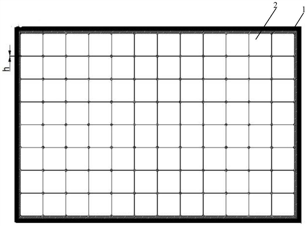
[0044]The coating carrier includes a carrier body 1 and a plurality of placement parts 2 for containing silicon wafers, and the placement parts 2 are evenly distributed along the longitudinal and transverse directions of the carrier body;

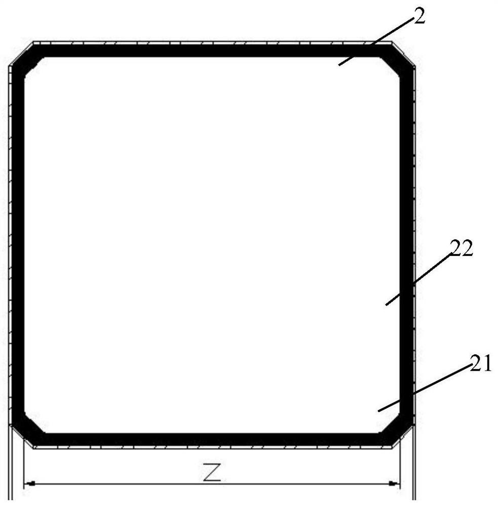
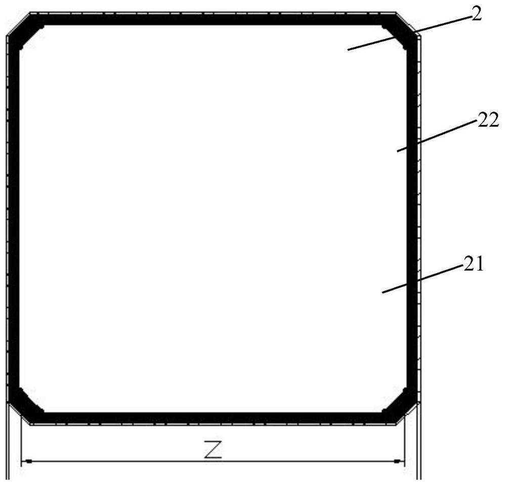
[0045] The placing part 2 includes a first frame body 22 and a second frame body 21, and the first frame body 22 is arranged outside the second frame body 21;

[0046] A plurality of support points 23 are oppositely arranged on the inner wall of the second frame body 21 .

[0047] In one embodiment, support points 23 are set at the inner four corners of the second frame body 21 or support points 23 are set at the opposite corners, the distance between the two opposite inner side walls of the second frame body 21 is Z, and the side length of the silicon wafer is A. Z≤A-0.2mm. If it exceeds the range value defined above, it will easily cause leakage of the battery device.

[0048] In one embodiment, when the support points 23 are set on the...

Embodiment 2

[0059] A method for increasing the TCO coating area of ​​a heterojunction solar cell comprising the following steps:

[0060] (1) Perform texturing treatment on N-type monocrystalline silicon wafers with a thickness of 180 μm to form a pyramid textured surface, remove impurity ions and clean the surface;

[0061] (2) Utilizing plasma chemical vapor deposition to prepare double intrinsic amorphous silicon layers on the front and back sides of the crystalline silicon wafer obtained in step (1);

[0062] (3) Prepare a doped amorphous silicon layer on the double-sided intrinsic amorphous silicon layer; one side of the doped amorphous silicon layer is doped with P to form N-type doped amorphous silicon, and the other side is doped with B to form P-type doped Heteromorphic silicon;

[0063] (4) Place the silicon chip made in step (3) on the placement part 2 of the coating carrier, and then prepare a double-sided conductive film layer and a mask area on the doped amorphous silicon l...


PUM


Abstract

The invention discloses a film coating carrier which comprises a carrier body and a plurality of placing parts for containing silicon wafers, wherein the placing parts are evenly distributed in the longitudinal direction and the transverse direction of the carrier body; each placing part comprises a first frame body and a second frame body, and the first frame body is arranged on the outer side of the second frame body; a plurality of supporting points are oppositely arranged on the inner side wall of the second frame body; the invention also discloses a method for increasing the TCO coating area of the heterojunction solar cell. The method comprises the following steps: (1) texturing and cleaning a crystal silicon wafer; (2) preparing a double-intrinsic amorphous silicon layer on the front surface of the crystal silicon wafer, and then preparing a double-doped amorphous silicon layer; (3) placing the prepared silicon wafer of the double-doped amorphous silicon layer on the placing part of the coating carrier, and then preparing a conductive thin film layer and a mask region on the double-doped amorphous silicon layer respectively; (4) forming a metal electrode on the conductive film layer in a silk-screen printing manner. When the coating carrier is applied to a subsequent coating method, the TCO coating area can be increased.

Description

technical field [0001] The invention relates to the technical field of solar energy, and more specifically relates to a coating carrier and a method for increasing the TCO coating area of ​​a heterojunction solar cell using the same. Background technique [0002] At present, with the development of solar cell technology, more and more attention has been paid to the development of high-efficiency cells. Among them, the silicon-based heterojunction solar cell (HJT cell) passivated by the intrinsic layer of amorphous silicon (a-Si:H(i)) is one of the key research directions. As we all know, silicon-based heterojunction solar cells not only have high conversion efficiency and high open circuit voltage, but also have low temperature coefficient, no light-induced degradation (LID), no electrical degradation (PID), low preparation process temperature, Short technological process and other advantages. In addition, while ensuring high conversion efficiency, the thickness of silicon...

Claims


Application Information

Patent Timeline
IPC IPC(8): H01L21/673H01L31/18H01L31/20C23C14/50C23C16/458
CPCH01L21/67326H01L31/1884H01L31/202C23C14/50C23C16/4581Y02E10/50Y02P70/50
Inventor 黄金王继磊杨立友白焱辉鲍少娟杨骥李莎贾慧君郭磊孔青青
Owner 晋能光伏技术有限责任公司
Why Eureka
Try Eureka