A method for manufacturing a large-area zinc oxide nano-micro generator

A manufacturing method and large-area technology, applied in the manufacturing/assembly of piezoelectric/electrostrictive devices, circuits, electrical components, etc., can solve the problems of expensive equipment and small deposition area, and achieve low cost and large film-forming area. , The effect of large-area controllable production and processing

Active Publication Date: 2017-05-10
NANJING YIDEGUAN ELECTRONICS TECH +1
View PDF5 Cites 0 Cited by
  • Summary
  • Abstract
  • Description
  • Claims
  • Application Information

AI Technical Summary

Problems solved by technology

The high plasma energy of PLD can increase the migration energy of atoms along the substrate surface, so that the thin film grows preferentially in the c-axis direction but the deposition area is small
Magnetron sputtering can realize the preparation of large-area piezoelectric materials, but the equipment is expensive

Method used


Image

  • A method for manufacturing a large-area zinc oxide nano-micro generator
  • A method for manufacturing a large-area zinc oxide nano-micro generator
  • A method for manufacturing a large-area zinc oxide nano-micro generator

Examples


Embodiment 1

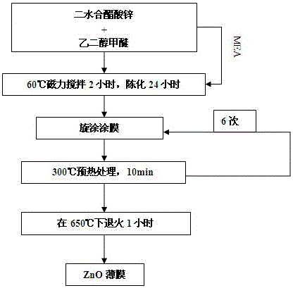
[0040] Example 1 Preparation of large-area ZnO thin films by sol-gel method

[0041] The preparation of large-area ZnO thin films by sol-gel method comprises the following steps:

[0042] 1) Preparation of sol solution: Mix 3.8412g zinc acetate dihydrate with 50ml ethylene glycol methyl ether to obtain a 0.35mol / L zinc acetate dihydrate ethylene glycol methyl ether solution, then add 1.4ml ethanolamine, and use magnetic The stirrer was fully stirred for 2 hours under the condition of 60°C water bath, and the solution was colorless and transparent. Aging at room temperature for 24 hours to obtain a sol solution;

[0043] 2) Cleaning of the substrate: Clean the 6-inch Si silicon wafer with an acetone solution in an ultrasonic cleaner for 30 minutes, then use ethanol for 30 minutes, then deionized water for 15 minutes, and then use HF: deionized water = 1:10 (volume than) the prepared dilute hydrofluoric acid solution to soak the substrate for 10 minutes, rinse it with deionize...

Embodiment 2

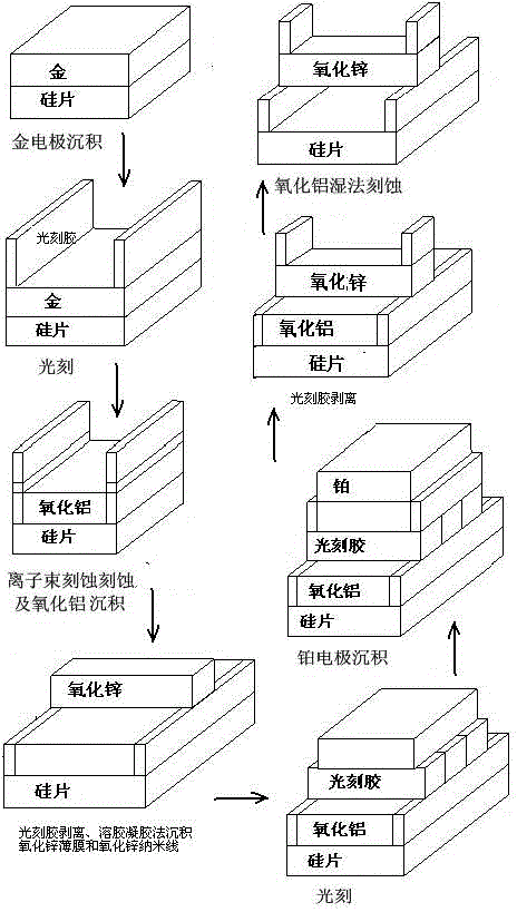
[0051] Embodiment 2 The manufacturing method of large-area ZnO nano-micro generator is characterized in that it comprises the following steps:

[0052] Step 1. Deposit Au electrodes on the cleaned 6-inch Si (100) substrate by electron beam evaporation deposition method; set the rate to 3 angstroms per second, select the high voltage as 600V, set the current to 300-350mA, and power to 180 watts ;

[0053] The second step is to spin coat the photoresist, and spin the Suzhou Ruihong RZJ-304 positive photoresist on the homogenizer at a low speed of 500rpm for 5s, and a high speed of 3000rpm for 30s. Using an ABM lithography machine to expose for 8s, the light intensity is 15mw / cm 2 ;The development time of photoresist depends on the development effect, and the development time depends on the development effect, generally between 8-15 seconds, forming a side wall structure in the Y direction;

[0054] In the third step, the Au without photoresist protection is etched away by ion ...


PUM


Abstract

A large area manufacturing method for zinc oxide nano micro generators comprises depositing a gold electrode on a substrate; coating photoresist in a spinning mode to form into a photoresist nano micro wire structure in the Y direction; etching gold electrode materials which are free of photoresist protection through ion beam etching, depositing hard mask material, namely aluminum oxide and etching aluminum oxide materials on the lateral wall to enable the photoresist to be exposed; stripping the photoresist and aluminum oxide on the photoresist through acetone and depositing a zinc oxide film through a sol-gel method; performing photoresist stripping through the ion beam etching and the acetone to form into zinc oxide nano wires; coating photoresist in a spinning mode and exposing the zinc oxide nano wires at two ends after exposure and forming; depositing a platinum electrode through electron beam evaporation, stripping the photoresist through the acetone and etching the aluminum oxide to form into a piezoelectric nano generator structure; exposing the piezoelectric nano generator to a vibration source to generate piezoelectric conversion and nano micro piezoelectric power generation. The large area manufacturing method for the zinc oxide nano micro generators achieves large area controllable production and manufacture of the low cost high mechanical energy to electric energy conversion nano generators.

Description

technical field [0001] The invention belongs to the field of manufacturing nanomaterials and nanodevices, and in particular relates to a method for manufacturing large-area zinc oxide nano-micro generators. Background technique [0002] Piezoelectric nanopower generation is a solution for sensor micropower in sensor networks. Chemically synthesized ZnO vertical piezoelectric nanowires can convert vibrational mechanical energy into electrical energy, achieving a peak voltage of 1.26 V and a peak power of 2.7 mW / cm 3 Output. The advantage of piezoelectric nanowires is high sensitivity and the ability to extract energy from sufficiently small natural sources. Although large piezoelectric potentials can also be observed on other non-ZnO nanowires, ZnO nanowires with both semiconducting and piezoelectric properties can complete the efficient conversion of mechanical energy to electrical energy. Conventional piezoelectric materials, such as PZT, are usually insulators. Althoug...

Claims


Application Information

Patent Timeline
Patent Type & Authority Patents(China)
IPC IPC(8): H01L41/39H01L41/318
Inventor 章伟高志强王瑞秦薇薇李涛许泳杨楠蔡依晨李雨桐徐玫瑰
Owner NANJING YIDEGUAN ELECTRONICS TECH
Why Eureka
Try Eureka