

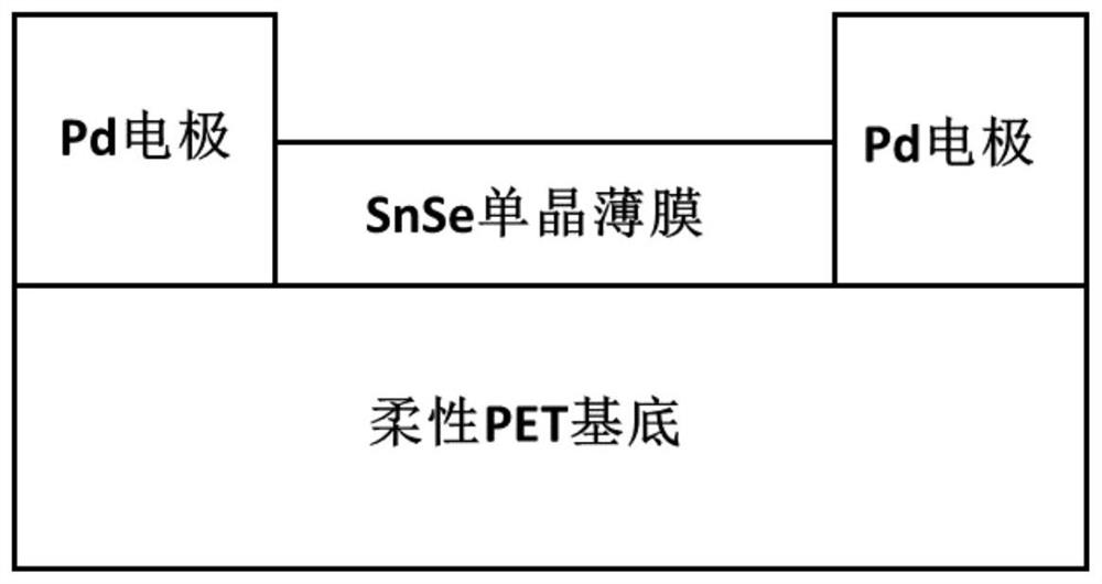
Flexible single crystal film photoelectric detector and preparation method thereof
A technology for photodetectors and single crystal thin films, applied in chemical instruments and methods, electrical components, single crystal growth, etc., can solve the problems of thin films that cannot be peeled and transferred, form flexible devices, and increase device costs. The effect of control, large film forming area and low manufacturing cost
- Summary
- Abstract
- Description
- Claims
- Application Information
AI Technical Summary
Problems solved by technology
Method used
Image

Examples
Embodiment 1
[0040] The preparation method is as follows:
[0041] The first step, NaCl crystal surface cleaning step
[0042] Select NaCl crystals and purge the surface with dry nitrogen;
[0043] Put the purged NaCl crystal into the tray, put it into the plasma cleaning chamber, and pump the cleaning chamber to a vacuum state of 3Pa, pass in Ar inert gas, adjust the air pressure to one-tenth of the atmospheric pressure, and use the plasma backsputtering technology. Under the conditions of 25°C and a constant 120W backsputtering power, the surface of the NaCl crystal is bombarded with plasma, and the ion bombardment cleaning time is 30 minutes. After the cleaning is completed, take it out;
[0044] The second step, thin film layer surface deposition step
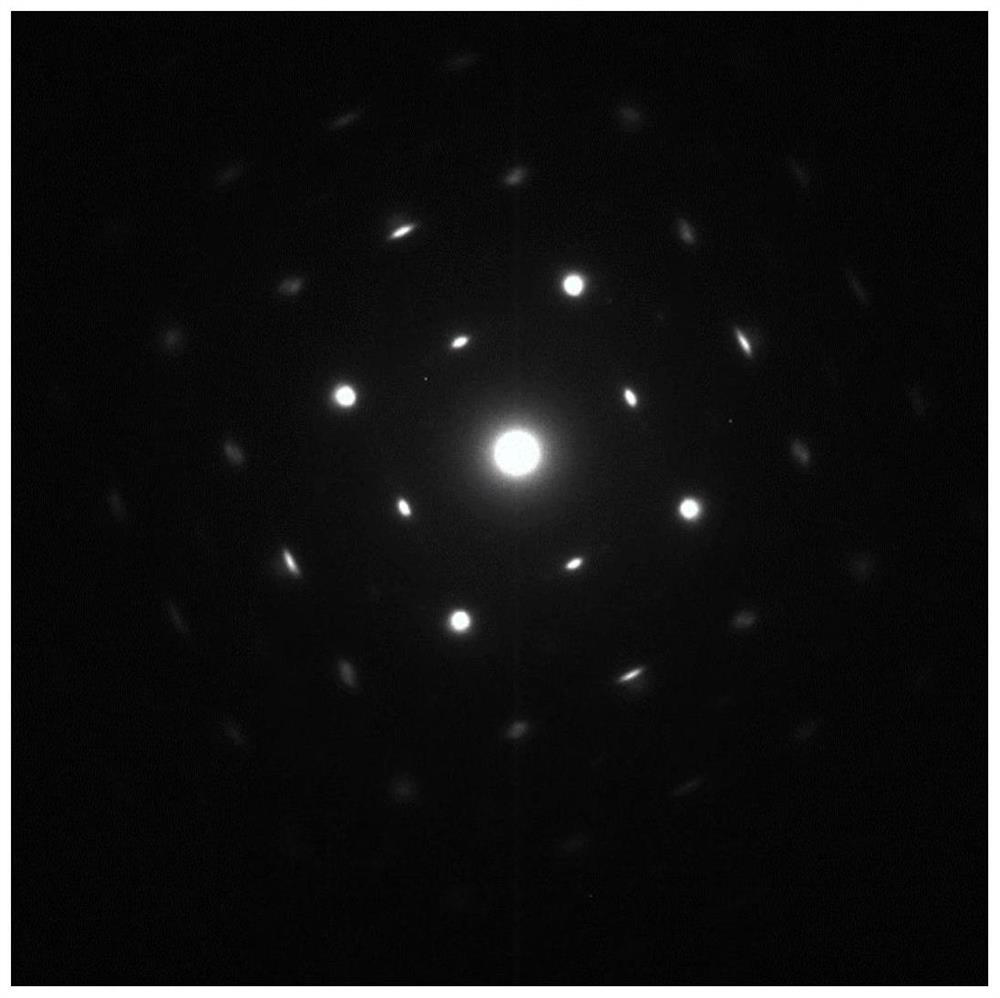
[0045] Transfer the ion-cleaned NaCl crystal into the sputtering chamber, and pump the sputtering chamber to 5×10 -4 Pa high vacuum, adjust the temperature of NaCl crystal to 400°C, adjust the argon gas pressure to 1.0Pa, use DC magn...
Embodiment 2
[0058] The material preparation method and steps are all the same as in Example 1.
[0059] Only in the second step, adjust the film thickness to 5 nm by adjusting the sputtering time.
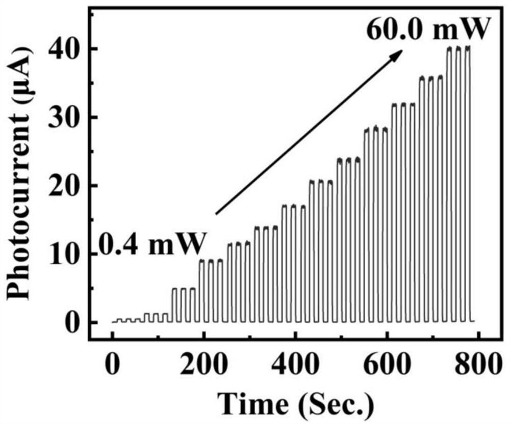
[0060] Product performance test results:
[0061] After testing, the responsivity value of the prepared flexible single crystal SnSe thin film material to 1550nm laser is 3.1A / W.
Embodiment 3
[0063] The material preparation method and steps are all the same as in Example 1.
[0064] Only in the second step, adjust the film thickness to 50 nm by adjusting the sputtering time.
[0065] Product performance test results:
[0066] After testing, the responsivity value of the prepared flexible single crystal SnSe thin film material to 1550nm laser is 3.8A / W.
PUM
| Property | Measurement | Unit |
|---|---|---|
| thickness | aaaaa | aaaaa |
| thickness | aaaaa | aaaaa |
| thickness | aaaaa | aaaaa |
Abstract
Description
Claims
Application Information