Method for preparing thin film material of binary rare earth compounds

A technology of rare earth compounds and thin film materials, applied in metal material coating process, ion implantation plating, coating and other directions, can solve the problems of limited quantity, difficult control, small ion beam current of rare earth elements, etc., to achieve high-efficiency and high-quality growth, The effect of improving uniformity and high melting point

Inactive Publication Date: 2006-07-05
INST OF SEMICONDUCTORS - CHINESE ACAD OF SCI
View PDF0 Cites 0 Cited by
  • Summary
  • Abstract
  • Description
  • Claims
  • Application Information

AI Technical Summary

Problems solved by technology

Although as early as 1995, people began to use low-energy double ion beam deposition method to prepare rare earth thin films, such as cerium oxide (CeO 2 ) thin films, but so far this method has not really become practical and widely promoted. The reasons for the analysis mainly include the following aspects: 1) Most of the original low-energy dual ion beam deposition methods use Freeman (Freeman) type solids Ion source, utilizes rare earth oxide as the raw material that produces rare earth element ion, and produces the working atmosphere of rare earth element chloride with the chlorination reaction in carbon tetrachloride gas to produce rare earth element ion, but because under the working pressure of ion source (10 -3 Pa to 10 -2 Pa), the amount of the carbon tetrachloride reaction gas that feeds is limited, and the rare earth oxide with high melting point and good stability is also easy to operate at a higher Freeman type ion source operating temperature (sometimes more than 800 ° C). Sintering and hardening, so only a small amount of rare earth chloride can be generated. The working atmosphere enters the arc chamber of the ion source for ionization, and the generated rare earth element ion beam current is small, and the film deposition efficiency is low; 2) The original low-energy dual ion beam deposition method , there is also an attempt to directly use rare earth chlorid

Method used


Image

  • Method for preparing thin film material of binary rare earth compounds
  • Method for preparing thin film material of binary rare earth compounds
  • Method for preparing thin film material of binary rare earth compounds

Examples


specific Embodiment 1

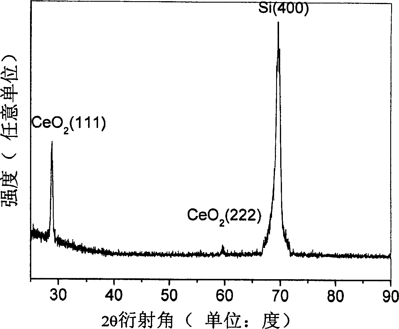
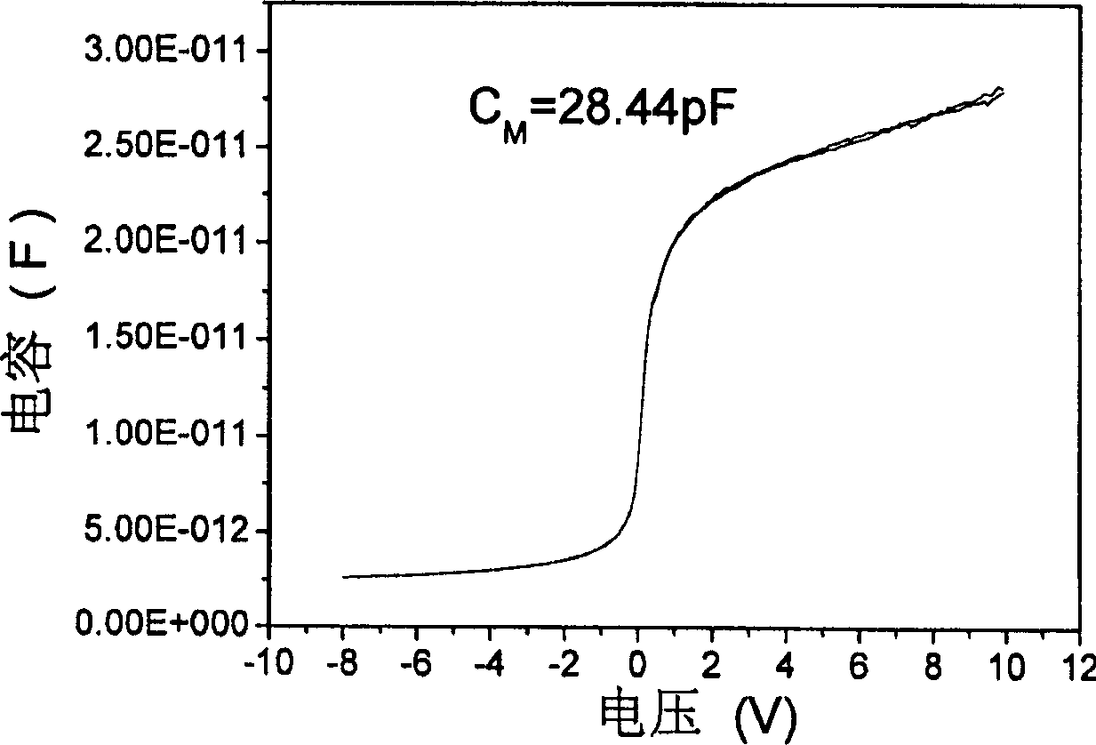
[0094] The scale of ultra-large-scale integrated circuits (ULSI) continues to increase, making the feature size of devices continue to decrease, which requires a new ideal high-dielectric material to replace the SiO commonly used in MOS devices. 2 materials, some binary rare earth oxide materials, such as cerium oxide (CeO 2 ) thin film, in addition to having a high dielectric constant and a good match with the silicon lattice, it also has good thermal stability. However, because most of these rare earth oxide materials have characteristics such as difficulty in purification and high melting point, it is difficult to prepare high-purity high-quality thin films by using the usual material growth technology. High-purity and high-quality rare earth cerium oxide (CeO 2 ) film, and the relevant experimental parameters and results are shown in Table 2. Because the present invention adopts low-cost anhydrous cerium chloride (CeCl 3 )) material is used as the raw material of the Be...

specific Embodiment 2

[0096] In recent years, the research on the luminescent properties of binary rare earth oxide materials has also attracted people's attention. Through the study of the luminescent mechanism of binary rare earth oxides, to grasp its mechanism and law, it can be used for rare earth oxides on silicon substrates. Optical applications of thin films, such as light sources, displays, imaging, optoelectronic devices, detection of radiation fields, and recording of radiation doses, lay the foundation for applications. The present invention utilizes the mass-separated low-energy dual ion beam deposition method to successfully prepare the rare earth gadolinium oxide (Gd 2 o 3 ) film material (see Figure 4 ), and for the first time in Gd 2 o 3 Four luminescence peaks were simultaneously found in the film sample (see Figure 5 ), this result is in good agreement with the "singlet-triplet exchange interaction" model, but there is no report of four luminescence peaks appearing at the sa...

specific Embodiment 3

[0098] Diluted magnetic semiconductor materials can simultaneously utilize the charge and spin properties of electrons, which is the basis for the future realization of quantum computing. However, it is difficult to obtain materials with room temperature ferromagnetism and high saturation magnetization, which restricts its wide application and promotion. In recent years, the use of magnetic rare earth elements to prepare high Tc ferromagnetic dilute magnetic semiconductor materials has gradually attracted people's attention. Process is difficult to achieve high solubility in semiconductor materials. The present invention utilizes the mass purification and energetic ion deposition functions of the low-energy ion beam deposition technology to obtain the magnetic rare earth element gadolinium (Gd + ) ions, producing Gd + The relevant experimental parameter of ion is referring to table 3, utilizes the magnetic rare earth element gadolinium (Gd) that the method of the present inv...


PUM


Abstract

This invention provides a preparation for binary rare earth compound thin films. A low-energy double ion beam deposition apparatus is adopted for its function of mass separation and characteristics of energetic ion deposition, and rare earth chlorides of which purity is not highly required serve as raw materials for I beam of Bonus solid ion source to give out an isotopic pure low-energy rare earth ion beam, which with another isotopic pure low-energy ion from II beam of Bonus gaseous ion source is deposited alternately in ultravacuum cultivation room. By exactly controlling the energy of the isotopic pure low-energy ions, beam shape, beam flux, beam proportion and growing temperature, deposition and low-temperature epitaxy of binary rare earth compounds which have high temperatures and are difficult to purify and easy to oxidized can be realized. A wide variety of rare earth thin films can be prepared according to this invention and the technique is convenient to modulate and optimized, which is economical to manufacture rare earth thin films used in semiconductor technology and some other fields.

Description

technical field [0001] The invention relates to the technical field of semiconductors, in particular to a method for preparing and growing binary rare earth compound thin film materials using mass-separated low-energy dual ion beam deposition equipment. Background technique [0002] Binary rare earth compound thin films are an important part of new functional materials, and are currently widely used in various fields. In particular, with the tremendous development of electronic information technology in recent years, the development and application of such materials in microelectronics, optoelectronics and magnetoelectronics in the field of semiconductors has attracted more and more attention. For example, some rare earth oxide films with high dielectric constants (such as cerium oxide (CeO 2 ), yttrium oxide (Y 2 o 3 ), etc.) are likely to replace silicon dioxide (SiO2) commonly used in microelectronics technology 2 ), become a new type of gate dielectric insulating mat...

Claims


Application Information

Patent Timeline
IPC IPC(8): C23C14/48C23C14/06C23C14/54
Inventor 杨少延柴春林刘志凯周建平陈诺夫王占国
Owner INST OF SEMICONDUCTORS - CHINESE ACAD OF SCI
Why Eureka
Try Eureka