Food processing method and device
A food processing and food technology, applied in the direction of food electrical processing, milking equipment, dairy products, etc., to achieve the effect of low voltage, low profile, and reduced electron energy flow state
- Summary
- Abstract
- Description
- Claims
- Application Information
AI Technical Summary
Problems solved by technology
Method used
Image
Examples
Embodiment 1
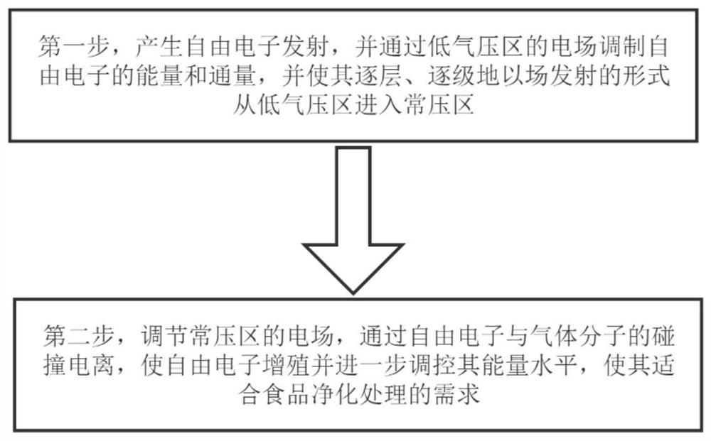
[0069] A food processing method, comprising the steps of:
[0070] In the first step, about 5×10 -3 The low pressure environment of Pa, the manufacturing average field strength is about 2×10 6 V / m free electron accelerating electric field, the manufacturing average field strength is about 8×10 5 The free electron collision process of V / m modulates the electric field, and in the electric field modulation during the free electron collision process, the normal pressure condition of the food is maintained. Under the above conditions, the cathode material obtains the Joule heat of the external circuit as the cathode of the field emission excitation circuit. Under the action of the electric field, the electrons escape from the surface of the cathode material and enter the low-pressure environment to become free electrons, adjusting the field of the free electron acceleration electric field Strong, according to calculations, the energy obtained by the acceleration of free electrons...
Embodiment 2
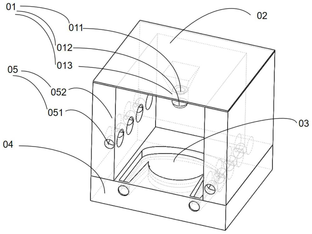
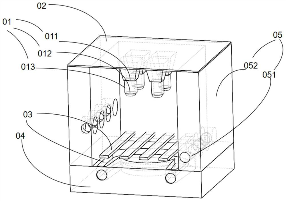
[0076] A free electronic food purification device, including the following components: low-energy electron source 01, deployment control component 02, electric field regulation function structure 03, food carrying component 04, wherein,
[0077] The low-energy electron source 01 includes a free electron emission structure 011, a multi-level field emission electron window 012, a vacuum packaging structure 013,
[0078] There is a gap of 1 mm between the free electron emission structure 011 and the multi-level field emission electron window 012, which is maintained by a perforated quartz round platform. The vacuum packaging structure 013 is assembled from a dielectric material cavity and a flange plate, with a diameter of about 32 mm, the gap between the free electron emission source 011 and the field emission electron window 012 is achieved and maintained by a mechanical pump and a molecular pump to form a 1×10 -3 The low pressure environment of Pa,
[0079] The free electron ...
Embodiment 3
[0091] A free electronic food purification device, including the following components: low-energy electron source 01, deployment control component 02, electric field regulation function structure 03, food carrying component 04, wherein,
[0092] The low-energy electron source 01 includes a free electron emission structure 011, a multi-level field emission electron window 012, a vacuum packaging structure 013,
[0093] There is a gap of about 10 mm between the free electron emission structure 011 and the multi-level field emission electron window 012, which is maintained by a perforated quartz round platform. The vacuum packaging structure 013 is formed by welding a ceramic cavity with a Kovar alloy and a metal packaging plate, with a diameter of About 32 mm, the gap formation between the free electron emission source 011 and the field emission electron window 012 is achieved and maintained by the getter below 1×10 -3 Pa low pressure environment,
[0094] The free electron emi...
PUM
| Property | Measurement | Unit |
|---|---|---|
| The average diameter | aaaaa | aaaaa |
| Wall thickness | aaaaa | aaaaa |
| Average height | aaaaa | aaaaa |
Abstract
Description
Claims
Application Information


