Ferromagnetic silicon carbide crystal and preparation method thereof

A silicon carbide and ferromagnetic technology, which is applied in the field of ferromagnetic silicon carbide crystal and its preparation, and achieves the effects of high surface quality, uniform P-type elements, and low basal plane dislocation density

Active Publication Date: 2022-07-12
SICC CO LTD
View PDF0 Cites 0 Cited by
  • Summary
  • Abstract
  • Description
  • Claims
  • Application Information

AI Technical Summary

Problems solved by technology

With the continuous development of information technology and the rapid improvement of processing and transmission speeds, the existing semiconductor integrated circuits are difficult to meet people's needs

Method used


Image

  • Ferromagnetic silicon carbide crystal and preparation method thereof
  • Ferromagnetic silicon carbide crystal and preparation method thereof
  • Ferromagnetic silicon carbide crystal and preparation method thereof

Examples


Embodiment 1

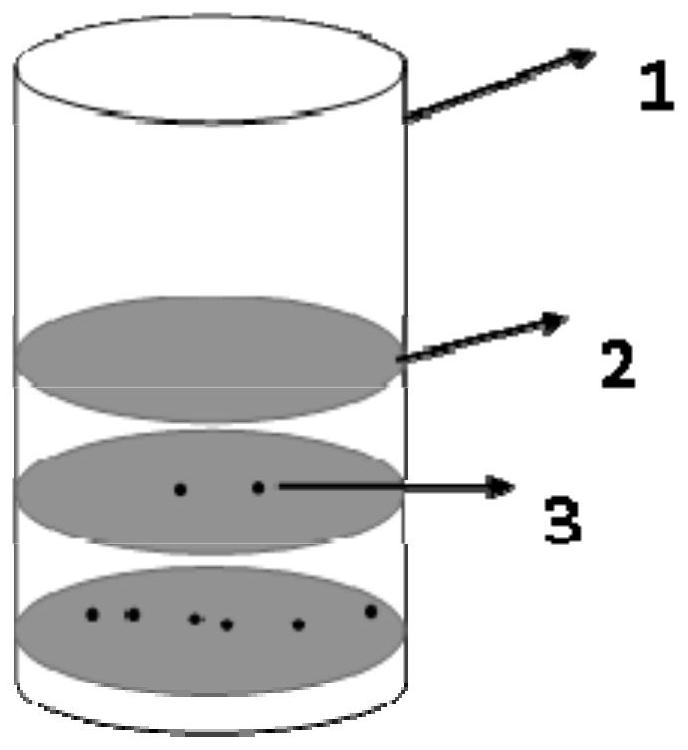
[0077] by figure 1 The illustrated embodiment of the 3-piece silicon carbide wafer is intended to illustrate the preparation method of the ferromagnetic silicon carbide crystal of the present application, but is not limited to the 3-piece silicon carbide wafer.

[0078]As an embodiment, the preparation method of ferromagnetic silicon carbide crystal comprises the following steps:

[0079] 1) Assembly steps: use medium frequency induction heating to grow crystals, and assemble the crucible before heating. The specific assembly is to adopt a layered charging method, and the boiling point (decomposition point) of Al with a temperature of 2200 ° C is assembled. 4 C 3 0.3g is placed between the upper and middle silicon carbide wafers, and 0.6g is placed between the middle and lower layers; the thicknesses of the upper silicon carbide wafer, the middle silicon carbide wafer, and the lower silicon carbide wafer are 500 μm, 450 μm, and 400 μm in sequence;

[0080] 2) Crystal growth:...

Embodiment 2

[0089] The difference between this example and Example 1 is that the Al in the raw material is adjusted 4 C 3 The concentration of doped aluminum ions and the generated holes in the obtained silicon carbide crystals were tested respectively, and the ferromagnetic silicon carbide crystals 2#-5# were obtained respectively, compared with the ferromagnetic silicon carbide crystals D1#-D2# , see Table 1 for details.

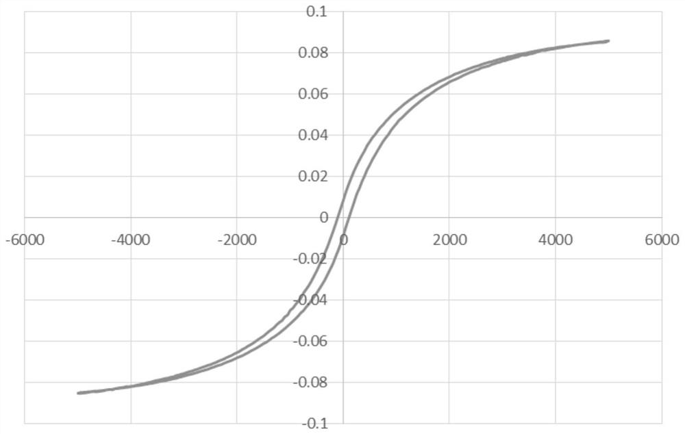
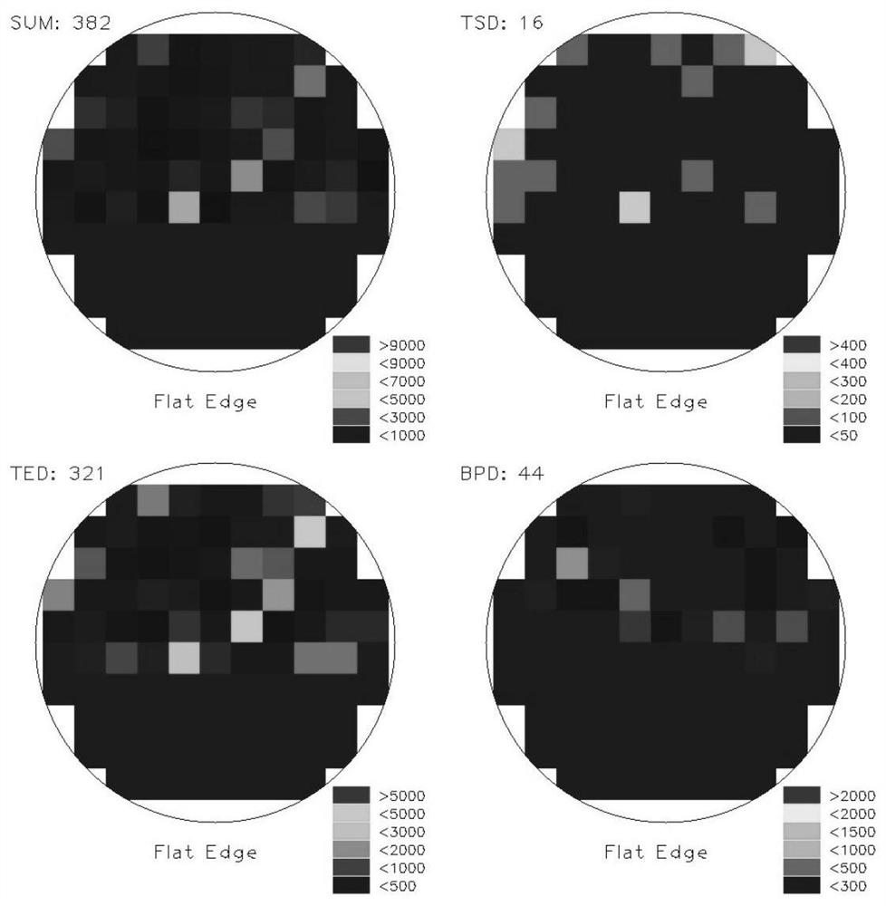
[0090] Test the obtained ferromagnetic silicon carbide crystals 1#-5# and comparative ferromagnetic silicon carbide crystals D1#-D2# respectively: magnetization curve (it can be judged whether it is ferromagnetic, saturation magnetization value), SIMS tests the aluminum ion concentration, Hall test for carrier concentration, resistivity and its distribution, and XRD.

[0091] Taking the test results of ferromagnetic silicon carbide crystal 1# as an example, the performance of the ferromagnetic silicon carbide crystal of the present application is described:

[0092...

Embodiment 3

[0101] The difference between the method for preparing ferromagnetic silicon carbide crystal in this embodiment and Embodiment 1 is:

[0102] 3) Regulation of holes: After 20h of growth in step c2, the nitrogen valve was opened to control the flow rate to 4sccm / min, and the flow was uniformly fed into the growth chamber for 30h until the end of the crystallization process, that is, the ferromagnetic silicon carbide crystal 6# was obtained.

[0103] Due to the difference between the nitrogen doping and the diameter of the silicon carbide atoms, the holes are introduced, and the introduced holes and the doping atoms work together to contribute to the ferromagnetism of the silicon carbide crystal.


PUM

PropertyMeasurementUnit
electrical resistivityaaaaaaaaaa

Abstract

The application discloses a ferromagnetic silicon carbide crystal and a preparation method thereof, belonging to the field of semiconductor materials. The ferromagnetic silicon carbide crystal has P-type doping ions and holes, and the concentration ratio of the P-type doping ions and holes is 1:3-10, so that the silicon carbide crystal is ferromagnetic P-type silicon carbide crystal. The silicon carbide crystal can reach a higher saturation magnetization at room temperature after passing through a magnetic field, so as to meet the requirement of ferromagnetic strength in the semiconductor silicon carbide crystal at room temperature.

Description

technical field [0001] The application relates to a ferromagnetic silicon carbide crystal and a preparation method thereof, belonging to the field of semiconductor materials. Background technique [0002] Semiconductor devices mainly use the charge properties of electrons to process and transmit information, while the information storage function is realized by using ferromagnetism, that is, the spin properties of electrons. With the continuous development of information technology and the rapid improvement of processing and transmission speeds, existing semiconductor integrated circuits cannot meet people's needs. If the charge and spin properties of electrons can be combined, there will undoubtedly be a huge technological breakthrough. Based on the realization of this ideal, spintronics came into being. [0003] As a third-generation semiconductor with excellent performance, SiC has good application prospects in the fields of high frequency and high power devices. If th...

Claims


Application Information

Patent Timeline
Patent Type & Authority Patents(China)
IPC IPC(8): C30B29/36C30B28/12C30B23/00
CPCC30B29/36C30B28/12C30B23/00
Inventor 张宁石志强姜彦鹏高超杨晓俐李博刘鹏飞
Owner SICC CO LTD
Why Eureka
Try Eureka