
Flexible single-crystal superconducting thin film, preparation method thereof and superconducting device

A technology of superconducting thin films and single crystals, which is applied in the manufacture/processing of superconducting devices, superconducting components, and superconducting devices, and can solve the problem of inability to obtain flexible and single-crystal superconducting thin films and the inability to withstand the growth temperature and other problems, to achieve excellent thermal stability, process controllability, and expand the effect of application range

Active Publication Date: 2021-12-24
NINGBO INST OF MATERIALS TECH & ENG CHINESE ACADEMY OF SCI
View PDF3 Cites 1 Cited by
  • Summary
  • Abstract
  • Description
  • Claims
  • Application Information

AI Technical Summary

Problems solved by technology

However, single crystal superconducting thin films often need to be grown at a temperature above 600°C and under relatively strict lattice matching conditions, and organic material substrates such as polyimide can neither withstand this growth temperature nor meet the requirements of epitaxy. Due to the lattice matching conditions required for growth, current single crystal superconducting films can only be grown on rigid single crystal substrates, so it is impossible to obtain flexible and single crystal superconducting films

Method used


Image

  • Flexible single-crystal superconducting thin film, preparation method thereof and superconducting device
  • Flexible single-crystal superconducting thin film, preparation method thereof and superconducting device
  • Flexible single-crystal superconducting thin film, preparation method thereof and superconducting device

Examples


preparation example Construction

[0027] Based on this, the preparation method of the flexible single crystal superconducting thin film provided by the application comprises the following steps:

[0028] S1, providing single crystal fluorophlogite;

[0029] S2, using the single crystal fluorine phlogopite as the substrate, the transition metal as the target, and nitrogen as the reaction gas, under vacuum conditions, adopting a reactive sputtering method to epitaxially grow a transition metal nitride film on the substrate, wherein, In the reactive sputtering method, the temperature of the substrate is 700°C-900°C, the flow rate of the nitrogen gas is 2sccm-10sccm, and the transition metal nitride thin film is a single crystal thin film;

[0030] S3, thinning the substrate with the transition metal nitride thin film, so that the thickness of the substrate is less than or equal to 50 μm, to obtain a flexible superconducting thin film.

[0031] In order to prevent the impurities on the fluorophlogopite placed in ...

Embodiment 1

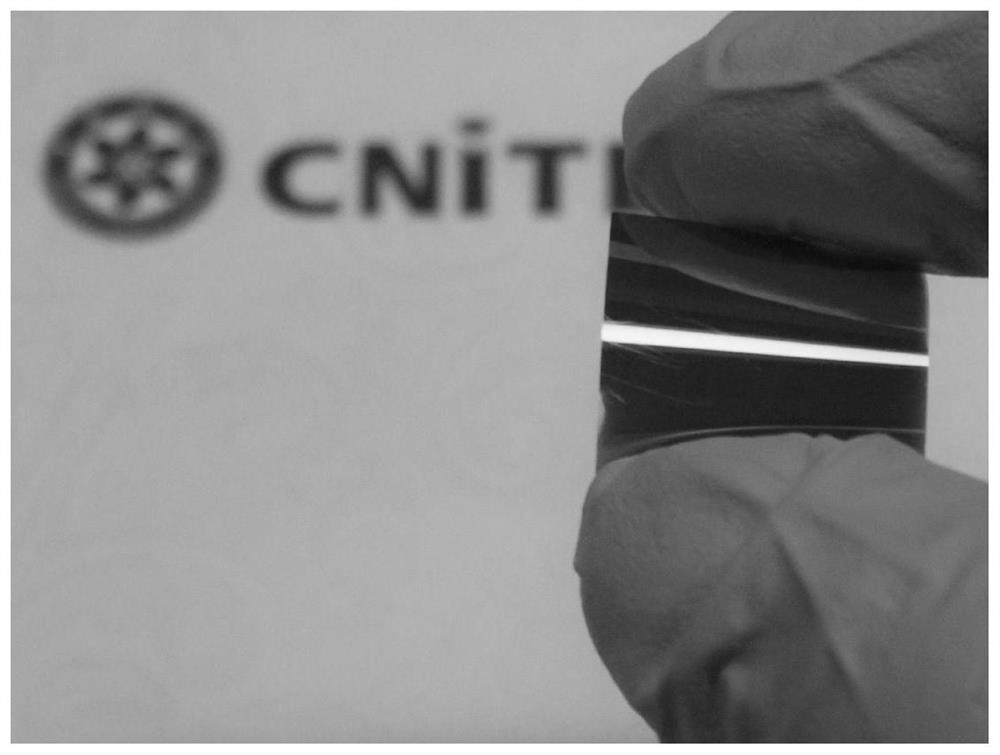
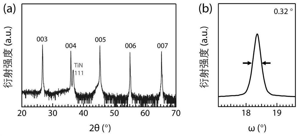
[0063] A titanium nitride thin film with a thickness of 80nm was prepared using fluorophlogopite as a substrate.

[0064] Provide 2cm*2cm fluorophlogopite as a substrate, use analytical grade acetone and alcohol solution to ultrasonically clean for 5 minutes, and blow dry with a nitrogen gun.

[0065] Load the cleaned substrate on the heating table in the sputtering chamber, and draw a vacuum until the vacuum degree reaches 1*10 - 6 Below Torr, turn on the power of the heating platform, set the temperature at 800°C, and bake the substrate for 30 minutes.

[0066] Introduce ultra-pure nitrogen gas into the sputtering chamber, and then start the mechanical pump and turbomolecular pump to evacuate to 1*10 -6 Torr, perform gas washing operation on the sputtering chamber and gas pipeline to remove impurity gas, and cycle 2 times. After the gas scrubbing, continue to draw vacuum until the background vacuum of the sputtering chamber reaches 1*10 -7 Torr ends pumping below.

[00...

Embodiment 2

[0073] A niobium nitride thin film with a thickness of 500nm was prepared using fluorophlogopite as a substrate.

[0074] Provide 3cm*3cm fluorophlogopite as the substrate, use analytical grade acetone and alcohol solution to ultrasonically clean for 10min, and blow dry with nitrogen gun.

[0075] Load the cleaned substrate on the heating table in the sputtering chamber, and draw a vacuum until the vacuum degree reaches 1*10 - 6 Below Torr, turn on the power of the heating platform, set the temperature at 800°C, and bake the substrate for 30 minutes.

[0076] Introduce ultra-pure nitrogen gas into the sputtering chamber, and then start the mechanical pump and turbomolecular pump to evacuate to 1*10 -6 Torr, wash the sputtering chamber and gas pipeline to remove impurity gas, and cycle 3 times. After the gas scrubbing, continue to draw vacuum until the background vacuum of the sputtering chamber reaches 1*10 -7 Torr ends pumping below.

[0077] Control the flow of ultra-pu...


PUM

PropertyMeasurementUnit
thicknessaaaaaaaaaa
thicknessaaaaaaaaaa
thicknessaaaaaaaaaa

Abstract

The invention relates to a preparation method of a flexible single-crystal superconducting thin film. The preparation method comprises the steps of providing single-crystal fluorine crystal mica; taking the single-crystal fluorine crystal mica as a substrate, transition metal as a target material and nitrogen as reaction gas, epitaxially growing a transition metal nitride thin film on the substrate by adopting a reaction sputtering method under a vacuum condition, and obtaining the superconducting thin film, wherein in the reaction sputtering method, the temperature of the substrate ranges from 700 DEG C to 900 DEG C, the flow rate of the nitrogen ranges from 2 sccm to 10 sccm, and the transition metal nitride thin film is a single-crystal thin film; and thinning the substrate with the transition metal nitride thin film so as to enable the thickness of the substrate to be less than or equal to 50 microns, and obtaining the flexible single-crystal superconducting thin film. According to the invention, the preparation of the superconducting thin film with both flexibility and single crystal property is realized. The invention also relates to a flexible single-crystal superconducting thin film and a superconducting device applying the flexible single-crystal superconducting thin film.

Description

technical field [0001] The invention relates to the field of superconducting thin film production, in particular to a flexible single crystal superconducting thin film, a preparation method thereof, and a superconducting device. Background technique [0002] Single crystal superconducting thin films can greatly improve the working quality of superconducting devices due to their excellent crystal quality and low defect density. However, single crystal superconducting thin films often need to be grown at a temperature above 600°C and under relatively strict lattice matching conditions, and organic material substrates such as polyimide can neither withstand this growth temperature nor meet the requirements of epitaxy. Due to the lattice matching conditions required for growth, current single crystal superconducting thin films can only be grown on rigid single crystal substrates, so it is impossible to obtain flexible and single crystal superconducting thin films. Contents of ...

Claims


Application Information

Patent Timeline
Patent Type & Authority Applications(China)
IPC IPC(8): C30B25/06C23C14/06C30B29/38H01L39/12H01L39/24H10N60/01H10N60/85
CPCC30B25/06C30B29/38C23C14/0641C23C14/0036H10N60/85H10N60/0241
Inventor 张如意曹彦伟宋洋彭邵勤毕佳畅裴宇娟
Owner NINGBO INST OF MATERIALS TECH & ENG CHINESE ACADEMY OF SCI
Learn More