Segmented injection self-clamping IGBT device and manufacturing method thereof

A segmented and device technology, which is applied in semiconductor/solid-state device manufacturing, semiconductor devices, electrical components, etc., can solve the problems of reducing on-resistance, increasing Miller capacitance, and degradation of breakdown characteristics, so as to improve conduction Increased resistance, reduced saturation current, and improved bearing capacity

Pending Publication Date: 2021-12-24
UNIV OF ELECTRONIC SCI & TECH OF CHINA +1
View PDF5 Cites 1 Cited by
  • Summary
  • Abstract
  • Description
  • Claims
  • Application Information

AI Technical Summary

Problems solved by technology

[0004] In order to improve the problems of large saturation current, poor short-circuit performance, degradation of breakdown characteristics, and increased Miller capacitance caused by deep trenches in the traditional CSTBT structure, the present invention proposes a split Segment-injected self-clamping IGBT structures such as figure 2 As shown, a trench structure with the same potential as the emitter and the same depth as the trench gate is introduced on the right side of the cell, and a high-concentration

Method used


Image

  • Segmented injection self-clamping IGBT device and manufacturing method thereof
  • Segmented injection self-clamping IGBT device and manufacturing method thereof
  • Segmented injection self-clamping IGBT device and manufacturing method thereof

Examples


Embodiment 1

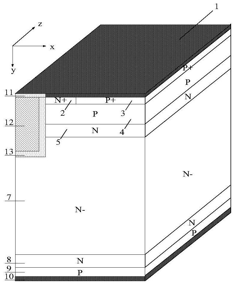
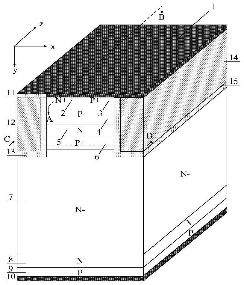
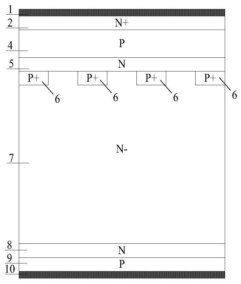
[0076] An embodiment of a segmented injection self-clamping IGBT device, its half-cell structure and the cross-section along the AB line and the CD line are as follows figure 2 , 3 , 4, including a collector metal 10, a P-type collector region 9, an N-type field stop layer 8, and an N-drift region 7 stacked sequentially from bottom to top, and a trench structure located above the N-drift region 7, The trench structure includes a gate dielectric layer 13, a polycrystalline gate electrode 12 in the gate dielectric layer 13, and a gate isolation dielectric layer 11 above the polycrystalline gate electrode 12;

[0077] It is characterized in that there is a P+ buried layer 6 and a separation gate structure above the N-drift region 7, and the separation gate structure includes a separation gate dielectric layer 15 and a polycrystalline separation gate electrode 14 in the separation gate dielectric layer 15;

[0078] Define the 3-dimensional direction of the device in a 3-dimension...

Embodiment 2

[0090] On the basis of Embodiment 1, a segmented implanted self-clamping IGBT device embodiment is proposed. The difference between this embodiment and Embodiment 1 lies in: the gap between any two adjacent P+ buried layers 6 along the Z direction The N-drift region 7 is replaced by a P-buried layer 16; the width of the P-buried layer 16 along the Z direction is less than or equal to the width of the P+ buried layer 6 along the Z direction; the concentration of the P-buried layer 16 is less than or equal to The concentration of the P-type base region 4 and the width of the P- buried layer 16 along the y direction are the same as the width of the P+ buried layer 6 along the y direction.

[0091] Its semi-cellular structure and the section along AB line and CD line are as follows Figure 5 , 6 As shown in , 7, a step is added between step 4 and step 5 in its manufacturing process: P-type buried layer 16 is formed by ion implantation of P-type impurities, and the rest of the pro...

Embodiment 3

[0104] On the basis of Embodiment 1, a segmented implanted self-clamping IGBT device embodiment is proposed. The difference between this embodiment and Embodiment 1 is that a super junction N column 17 and a super The super junction structure formed by junction P pillars 18. Its semi-cellular structure and the section along AB line and CD line are as follows Figure 8 , 9 , as shown in 10,

[0105] The introduction of the superjunction structure further reduces the conduction voltage drop of the device and increases the breakdown voltage of the device.


PUM


Abstract

The invention provides a segmented injection self-clamping IGBT and a manufacturing method thereof. A trench structure equipotential with an emitter is introduced to the right side of a cell, the P-type doped buried layers are introduced below an N-type charge storage layer, and the high-concentration P-type buried layers are distributed at intervals by changing an opening of a mask plate, so that the adverse effect of the high-concentration P-type buried layers on the threshold voltage when a device is conducted is improved, and the on-resistance is reduced. When the device is saturated, a self-biased PMOS structure is opened, and the electric potential of a CS layer is clamped at a lower value, so that the saturation current of the IGBT is reduced. The high-concentration P-type buried layers distributed at intervals can ensure that the PMOS structure is normally started under high collector voltage so as to clamp the potential of the CS layer, the saturation current is reduced, and the short-circuit capability of the device is improved. On the basis of a traditional trench IGBT process method, the P+ buried layers distributed in a segmented mode in a z direction can be achieved only by adding one mask, the process complexity is not increased, and implementation is easy.

Description

technical field [0001] The invention belongs to the technical field of power semiconductor devices, and relates to an insulated gate bipolar transistor (IGBT), in particular to a segmented injection self-clamping IGBT and a manufacturing method thereof. Background technique [0002] As a new type of power device, insulated gate bipolar transistor (IGBT) combines the gate electrode voltage control characteristics of metal oxide semiconductor field effect transistor (MOSFET) and the low on-resistance characteristics of bipolar junction transistor (BJT), with voltage control , large input impedance, small driving power, small on-resistance, high current density, low switching loss and high operating frequency, it is an ideal semiconductor power switching device, which is obtained in various power conversion, motor drive and power electronic devices. widely used. [0003] Since the advent of the IGBT, people have been working on improving the trade-off relationship between the ...

Claims


Application Information

Patent Timeline
IPC IPC(8): H01L29/06H01L29/739H01L21/331
CPCH01L29/7398H01L29/7397H01L29/66348H01L29/0684H01L29/0696Y02B70/10
Inventor 张金平肖翔张琨张波
Owner UNIV OF ELECTRONIC SCI & TECH OF CHINA
Why Eureka
Try Eureka