Nitrogen-containing compound and electronic component and electronic device using same
一种氮化合物、化合物的技术,应用在电气元件、电固体器件、电路等方向,能够解决发光效率降低、发光器件性能下降、寿命缩短等问题,达到提高玻璃化转变温度、改善稳定性、延长寿命的效果
- Summary
- Abstract
- Description
- Claims
- Application Information
AI Technical Summary
Problems solved by technology
Method used
Image
Examples
Synthetic example
[0121] Synthesis of intermediates
[0122]
[0123] To a dry and nitrogen-purged round-bottom flask, add 1-bromo-2-iodo-3-chlorobenzene (50.0 g, 157.5 mmol), phenylboronic acid (19.2 g, 157.5 mmol), tetrakis(triphenylphosphine) Palladium (9.1g, 7.8mmol), tetrabutylammonium bromide (2.5g, 7.8mmol), potassium carbonate (65.2g, 472.6mmol), toluene (400mL), ethanol (200mL), deionized water (100mL), With stirring, the temperature was raised to 75°C and kept for 8h; then the reaction mixture was cooled to room temperature, deionized water (200mL) was added, stirred for 15 minutes, the organic phase was separated, anhydrous magnesium sulfate was added to dry, and the solvent was removed under reduced pressure; The crude product was purified by silica gel column chromatography using dichloromethane / n-heptane (1:3) as mobile phase to obtain intermediate SM-D (35.8g, yield 85%).
[0124] To a dry and nitrogen-substituted round-bottomed flask, add SM-D (35.8g, 133.8mmol), tetrahydrof...
Embodiment 1
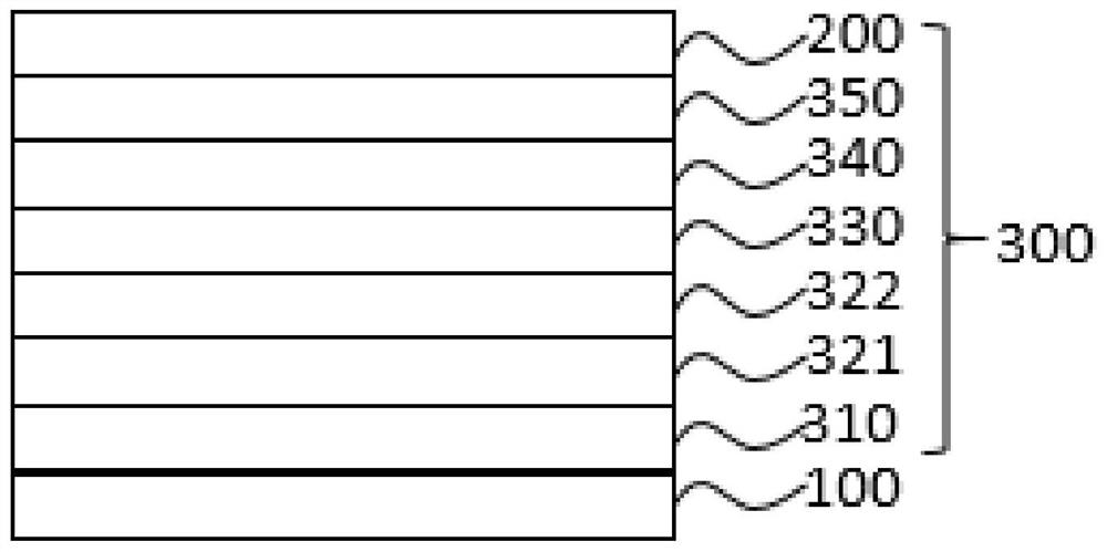
[0177] Embodiment 1: green organic electroluminescent device
[0178] The anode was prepared by the following process: the thickness of ITO was The substrate (manufactured by Corning) was cut into a size of 40mm × 40mm × 0.7mm, and it was prepared into an experimental substrate with cathode, anode and insulating layer patterns by using a photolithography process, using ultraviolet ozone and O 2 :N 2 Plasma surface treatment was performed to increase the work function of the anode (experimental substrate) and to remove scum.
[0179] F4-TCNQ was vacuum evaporated on the experimental substrate (anode) to form a thickness of The hole injection layer (HIL), and NPB is evaporated on the hole injection layer to form a thickness of hole transport layer.
[0180] Compound 1 was vacuum evaporated on the hole transport layer to form a thickness of electron blocking layer.
[0181] On the electron blocking layer, GH-n1:GH-n2:Ir(ppy) 3 Carry out co-evaporation with the ratio of...
Embodiment 2- Embodiment 40
[0185] When forming the electron blocking layer, the compounds shown in Table 12 were used instead of Compound 1 in Example 1, and an organic electroluminescent device was fabricated by the same method as in Example 1.
PUM
 Abstract
Description
Claims
Application Information


