
Composite structure AlN seed crystal for PVT and preparation and application thereof

A composite structure and seed crystal technology, which is applied in crystal growth, single crystal growth, single crystal growth, etc., can solve the problem that the processing accuracy such as warpage cannot be less than microns, affects the purity and quality of crystals, and reduces the diameter of crystals. speed and other issues to achieve the effect of improving the quality of crystal growth, reducing cracks and dislocations, and reducing the generation of pores

Pending Publication Date: 2022-01-21
ULTRATREND TECH INC
View PDF8 Cites 1 Cited by
  • Summary
  • Abstract
  • Description
  • Claims
  • Application Information

AI Technical Summary

Problems solved by technology

Compared with homoepitaxial technology, cracks and dislocations are mainly optimized by optimizing the temperature distribution around the seed crystal and reducing the radial temperature gradient. Stress, resulting in a large number of defects such as initial dislocations
At the same time, the reduction of the radial temperature gradient will reduce the rate of crystal diameter expansion and reduce the crystal growth efficiency.
The method of reducing the internal pores of the crystal can be to strengthen the adhesion between the seed crystal and the back support and minimize the gap between them, but it cannot be avoided well, and the machining accuracy such as warpage cannot reach the level of less than microns
In addition, there is also a solution through chemical bonding, but it will affect the purity and quality of the crystal

Method used


Image

  • Composite structure AlN seed crystal for PVT and preparation and application thereof
  • Composite structure AlN seed crystal for PVT and preparation and application thereof
  • Composite structure AlN seed crystal for PVT and preparation and application thereof

Examples


Embodiment 1

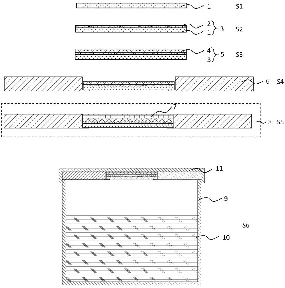
[0023] First, AlN seed crystals with a composite structure are prepared, as shown in the attached figure 1 As described above, it mainly includes the steps of: selecting an AlN single wafer 1 as an aluminum nitride seed wafer (S1), coating the surface of the aluminum nitride seed wafer with a back-sealing film 2 (S2), and coating an AlN thick film 4 on the back-sealing film to form a composite structure AlN seed crystal (S3). The AlN seed crystal of the composite structure is placed in the accessory tank (S4), the back cover metal sheet is added (S5), and the accessory tank is assembled on the top of the crucible for crystal epitaxial growth (S6). Attached below figure 1 , the specific steps of this embodiment are described in detail as follows:

[0024] 1) Step S1: A double-sided polished AlN single wafer is prepared as an aluminum nitride seed wafer 1 with a diameter of 51 mm. The thickness H0 of the seed wafer 1 is 0.5mm, and both sides are treated by chemical mechanical...


PUM

PropertyMeasurementUnit
surface roughnessaaaaaaaaaa
thicknessaaaaaaaaaa
thicknessaaaaaaaaaa

Abstract

The invention provides a composite structure AlN seed crystal for PVT, the AlN seed crystal sequentially comprises an aluminum nitride seed wafer, a back sealing film and an AlN thick film from top to bottom, the two faces of the aluminum nitride seed wafer are polished faces, and the roughness of the back face of the aluminum nitride seed wafer is smaller than 2 nm; the back sealing film is a combination of one or more layers of any one of W, Mo, Ta, WC, TaC, BN and diamond, and is formed on the back surface of the aluminum nitride seed wafer through a coating method; and the AlN thick film covers the back sealing film through a film coating method, and the thickness of the AlN thick film is 0.5-5 mm. The invention provides a method for preparing the composite-structure AlN seed crystal and application of the composite-structure AlN seed crystal in PVT epitaxial growth of an AlN crystal. The density of various defects (cracks, dislocations and air holes) can be effectively reduced, and the crystal growth quality is improved.

Description

technical field [0001] The invention relates to the technical field of semiconductor material preparation, in particular to a method for improving the quality of aluminum nitride crystals. Background technique [0002] For half a century, the development and application of the first and second-generation semiconductor electronic devices have reached their limits, and the third-generation semiconductor has attracted widespread attention in the field of modern science and technology because of its superior material properties. Aluminum nitride (AlN), as one of the representative materials of the third-generation semiconductors, has a band gap as high as 6.2eV, high breakdown field strength, high electron migration rate, and excellent thermal conductivity and radiation resistance. (LED), laser diode (LD), microwave radio frequency devices, high-temperature / high-power electronic devices are high-quality substrates, and have broad application prospects in semiconductor lighting, ...

Claims


Application Information

Patent Timeline
Patent Type & Authority Applications(China)
IPC IPC(8): C30B29/40C30B23/02C23C14/35C23C14/16
CPCC30B29/403C30B23/025C23C14/35C23C14/165
Inventor 吴亮黄嘉丽王琦琨雷丹李哲张刚赵寅廷
Owner ULTRATREND TECH INC
Learn More