Groove PiN type beta irradiation battery with gate electrode surface field and preparation method of groove PiN type beta irradiation battery
A gate electrode and surface field technology, applied in the field of microelectronics, can solve the problems of increasing the saturation current of PiN devices, enhancing the negative impact of surface recombination, and limiting energy conversion efficiency, so as to reduce the saturation current, reduce recombination, and weaken device surface recombination The effect of action
- Summary
- Abstract
- Description
- Claims
- Application Information
AI Technical Summary
Problems solved by technology
Method used
Image
Examples
Embodiment 1
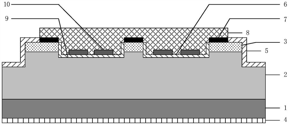
[0059] See figure 2 , figure 2 A schematic structural diagram of a grooved PiN type β-irradiated cell with a gate electrode surface field provided by an embodiment of the present invention. The irradiation battery includes: a PiN unit and a radioisotope unit located on the PiN unit.
[0060] PiN unit includes N-type doped 4H-SiC substrate 1, N-type doped 4H-SiC epitaxial layer 2, P-type doped 4H-SiC epitaxial layer 3, N-type ohmic contact electrode 4, isolation passivation layer 5, trench A trench passivation layer 6 , a P-type ohmic contact electrode 7 , several trench regions 9 and a gate electrode 10 .
[0061] Specifically, the shape of the PiN unit can be square or circular. When the PiN unit is square, its mesa area is 0.5×0.5cm~1.0×1.0cm; when the PiN unit is circular, its mesa area is Φ0.5cm ~Φ1.0cm; but the shape and area of the PiN unit are not limited to the above description, for example, the shape of the PiN unit can also be rectangle, trapezoid, etc.
[0...
Embodiment 2
[0106] On the basis of Example 1, please refer to Figure 6a-Figure 6m , Figure 6a-Figure 6m It is a process schematic diagram of a method for preparing a grooved PiN-type β-irradiated cell with a gate electrode surface field provided by an embodiment of the present invention. The preparation method comprises steps:
[0107] S1. Epitaxial growth of N-type doped 4H-SiC epitaxial layer 2 on N-type doped 4H-SiC substrate 1, see Figure 6a and Figure 6b .
[0108] First, the N-type doped 4H-SiC substrate 1 sample is cleaned to remove surface pollutants.
[0109] Then, use chemical vapor deposition CVD to epitaxially grow a layer with a doping concentration of 1×10 on the cleaned N-type highly doped 4H-SiC substrate 1 sample surface. 14 ~1×10 15 cm -3 N-type low-doped 4H-SiC with a thickness of 4.0-10.0 μm forms an N-type doped 4H-SiC epitaxial layer 2 .
[0110] S2. Epitaxial growth of P-type doped 4H-SiC epitaxial layer 3 on N-type doped 4H-SiC epitaxial layer 2, please...
Embodiment 3
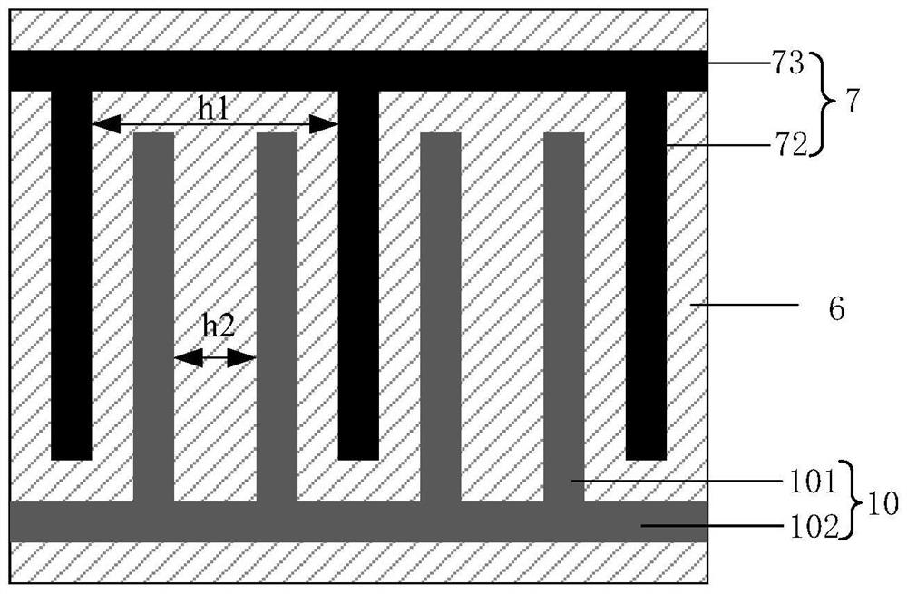
[0133] On the basis of Example 2, please combine Figure 4a and Figure 6a-Figure 6m , this embodiment takes a grooved silicon carbide PiN-type β-irradiated cell with finger-shaped distributed P-type regions and a gate electrode surface field as an example to illustrate its preparation method, wherein the cell area is 0.6×0.6 cm, and the groove The width is 405 μm, the width of the first vertical rectangular strip 72, the first horizontal rectangular strip 73, the second vertical rectangular strip 101, and the second horizontal rectangular strip 102, that is, the electrode width is 20 μm, and the number of the first vertical rectangular strip 72 is 14, The number of second longitudinal rectangular strips 101 in the gate electrode 10 is 195, 15 second longitudinal rectangular strips 101 are arranged between adjacent first longitudinal rectangular strips 72, and the distance between adjacent second longitudinal rectangular strips 101 is h2 is 5 μm, the number of the first horiz...
PUM
| Property | Measurement | Unit |
|---|---|---|
| thickness | aaaaa | aaaaa |
| thickness | aaaaa | aaaaa |
| thickness | aaaaa | aaaaa |
Abstract
Description
Claims
Application Information


