Preparation method of TopCon battery
A technology for batteries and semi-finished products is applied in the field of solar cells to achieve the effects of reducing costs, improving battery efficiency, and simplifying manufacturing processes
- Summary
- Abstract
- Description
- Claims
- Application Information
AI Technical Summary
Problems solved by technology
Method used
Image
Examples
preparation example Construction
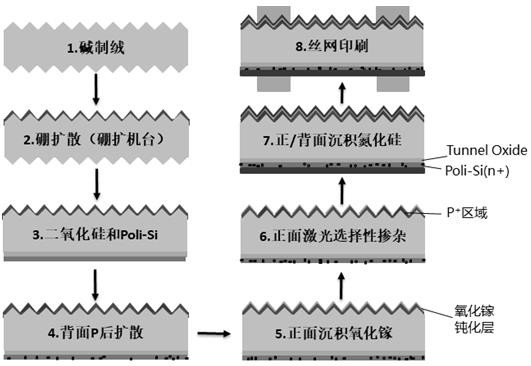
[0030] The invention provides a preparation method of a TopCon battery, comprising:
[0031] Provide a semi-finished product of the TopCon cell; the semi-finished product includes a silicon wafer, an emitter layer arranged on the front side of the silicon wafer, a tunnel oxide layer and a doped polysilicon layer arranged on the backside of the silicon wafer in sequence;
[0032] Deposit a gallium oxide passivation layer on the front side of the semi-finished product;
[0033] Selectively doping the front side of the semi-finished product with the gallium oxide passivation layer deposited by laser;
[0034] Deposit a front anti-reflection layer and a back anti-reflection layer on the front and back of the semi-finished product treated by selective doping respectively;
[0035] Electrodes are respectively prepared on the front and back of the semi-finished product on which the front anti-reflection layer and the back anti-reflection layer are deposited to obtain a TopCon batter...
Embodiment 1
[0056] This embodiment provides an N-type gallium oxide passivation front-side selective doping double-sided cell, which consists of a front-side light trapping and passivation layer: silicon nitride / gallium oxide; P-type emitter; P+ selective emitter composition.
[0057] The preparation method includes the following steps:
[0058] 1.1 Select an N-type silicon wafer with a resistivity of 1.5 Ω·cm for alkaline texturing cleaning, and the reflectivity after texturing is 10%.
[0059] 1.2 Carry out B diffusion, where BBr 3 N 2 The flow rate was 120 sccm, the advancing temperature was 900 °C, and the advancing time was 100 min to form a P-type diffusion layer with low surface concentration, and the diffusion square resistance was 120 Ω / sq.
[0060] 1.3 Remove the BSG and P+ layers on the back and sides by cleaning, and use LPCVD equipment to prepare SiO on the back 2 Tunneling layer, the thickness of the tunneling layer is 5 nm; 2 A Poli-Si layer is laminated on the layer w...
Embodiment 2
[0067] This embodiment provides an N-type gallium oxide passivation front-side selective doping double-sided cell. Compared with Embodiment 1, the thickness of gallium oxide in this embodiment is 1 nm.
[0068] The solar cell was prepared according to the preparation method in Example 1, and the test results showed that the open circuit voltage was 698V, the current was 11.02A, and the conversion efficiency was 23.10%.
PUM
| Property | Measurement | Unit |
|---|---|---|
| thickness | aaaaa | aaaaa |
| wavelength | aaaaa | aaaaa |
| thickness | aaaaa | aaaaa |
Abstract
Description
Claims
Application Information
 - R&D
- Intellectual Property
- Life Sciences
- Materials
- Tech Scout
- Unparalleled Data Quality
- Higher Quality Content
- 60% Fewer Hallucinations
Browse by: Latest US Patents, China's latest patents, Technical Efficacy Thesaurus, Application Domain, Technology Topic, Popular Technical Reports.
© 2025 PatSnap. All rights reserved.Legal|Privacy policy|Modern Slavery Act Transparency Statement|Sitemap|About US| Contact US: help@patsnap.com

