Process integration method for integrating high-voltage CMOS (complementary metal oxide semiconductor) in logic process

An integrated method and process technology, applied in the direction of electrical components, semiconductor/solid-state device manufacturing, circuits, etc., can solve problems such as STI depth should not be too deep, device failure, defects, etc., to improve doping uniformity, eliminate defects and positions Wrong, the effect of improving the withstand voltage performance

Pending Publication Date: 2022-03-25
SHANGHAI HUAHONG GRACE SEMICON MFG CORP
View PDF0 Cites 0 Cited by
  • Summary
  • Abstract
  • Description
  • Claims
  • Application Information

AI Technical Summary

Problems solved by technology

Although these thermal processes are completed before the logic device is fabricated, if the thermal process occurs after the shallow trench isolation (STI) of the logic process, a large stress will be formed in the active area, causing defects and dislocations in the active area. cause device failure
[0004] If the oxidation process of the thick gate silicon oxide of high-voltage CMOS is completed after STI, the oxidation speed in the edge region of STI is slow, resulting in uneven thickness of the gate oxide layer of high-voltage CMOS, and double peaks appear in the Id-Vg curve, forming a device The high leakage current phenomenon, Id is the drain current, Vg is the gate voltage
[0005] The low on-resistance of high-voltage CMOS requires that the depth of STI in its drift region should not be too deep, which is incompatible with the depth of STI in advanced logic technology

Method used


Image

  • Process integration method for integrating high-voltage CMOS (complementary metal oxide semiconductor) in logic process
  • Process integration method for integrating high-voltage CMOS (complementary metal oxide semiconductor) in logic process
  • Process integration method for integrating high-voltage CMOS (complementary metal oxide semiconductor) in logic process

Examples


Embodiment Construction

[0052] Such as figure 1 As shown, it is a flowchart of a process integration method for integrating a high-voltage CMOS in a logic process according to an embodiment of the present invention; as Figure 2A to Figure 2N Shown is a schematic diagram of the device structure in each step of the process integration method for integrating high-voltage CMOS in the logic process of the embodiment of the present invention; the operating voltage of the logic device in the process integration method for integrating high-voltage CMOS in the logic process of the embodiment of the present invention The operating voltage of CMOS, including the following steps:

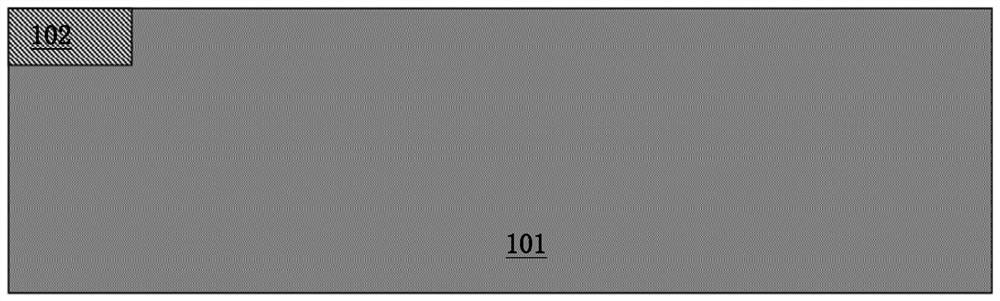
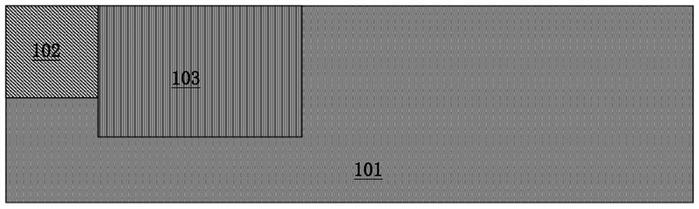
[0053] Step 1, such as Figure 2A As shown, the first channel region 102 doped with the second conductivity type is formed in the semiconductor substrate 101 in the selected region of the high voltage CMOS formation region 201 . The high voltage CMOS formation region 201 is in Figure 2C marked with curly brackets.

[0054] In th...


PUM


Abstract

The invention discloses a process integration method for integrating a high-voltage CMOS (Complementary Metal Oxide Semiconductor) in a logic process. The process integration method comprises the following steps of: 1, forming a first channel region of the high-voltage CMOS; step 2, forming a first drift region of the high-voltage CMOS; step 3, carrying out primary furnace tube hot drive-in; 4, forming a high-voltage gate oxide layer by adopting a first thermal oxidation process; 5, forming shallow trench isolation, wherein the depth of the first shallow trench isolation in the formation region of the high-voltage CMOS is smaller than that of the second shallow trench isolation in the formation region of the logic device; 6, completing a process before the formation process of the gate conductive material layer in the formation region of the logic device, and then forming the gate conductive material layer; and step 7, performing heavily doped source-drain injection of the first conductive type. According to the invention, the stress generated by the thermal process required by the high-voltage CMOS on the active region can be eliminated, so that the defects of the active region caused by the stress are eliminated, and the quality of the high-voltage gate oxide layer and the performance of the high-voltage CMOS are improved.

Description

technical field [0001] The invention relates to a method for manufacturing a semiconductor integrated circuit, in particular to a process integration method for integrating high-voltage CMOS in a logic process. Background technique [0002] High-voltage CMOS technology is the manufacturing process of screen display driver chips. Its characteristic is that high-voltage CMOS devices need to be integrated with logic technology to realize the organic combination of high-voltage drive and logic signal processing. [0003] Both the gate and the drain of a high-voltage CMOS device need to withstand high voltage, so a thick gate oxide layer, that is, a thick gate silicon oxide dielectric layer, is also required to have a relatively uniformly doped drain end drift region formed by a thermally pushed well, all of which require A large number of thermal processes are introduced into the process. Although these thermal processes are completed before the logic device is fabricated, if ...

Claims


Application Information

Patent Timeline
Patent Type & Authority Applications(China)
IPC IPC(8): H01L21/8238
CPCH01L21/823857H01L21/823878
Inventor 钱文生
Owner SHANGHAI HUAHONG GRACE SEMICON MFG CORP
Why Eureka
Try Eureka