Organic field effect transistor device and preparation method thereof

A transistor and organic field technology, applied in the field of organic field effect transistor devices and their preparation, can solve the problems of development limitations, low crystallinity of triazine covalent organic framework materials, etc., and achieve easy access, broadened application range, semiconductor performance Good results

Pending Publication Date: 2022-03-25
HEBEI UNIVERSITY OF SCIENCE AND TECHNOLOGY
View PDF0 Cites 1 Cited by
  • Summary
  • Abstract
  • Description
  • Claims
  • Application Information

AI Technical Summary

Problems solved by technology

Due to the high temperature required for the reaction, the monomers suitable for this type of reaction are limited, and the crystallinity of triazine covalent organic framework materials is low, the development and application of this type of covalent organic framework materials are limited.

Method used


Image

  • Organic field effect transistor device and preparation method thereof
  • Organic field effect transistor device and preparation method thereof
  • Organic field effect transistor device and preparation method thereof

Examples


Embodiment 1

[0055] This embodiment provides a method for preparing an organic field effect transistor device, the preparation method comprising the following steps:

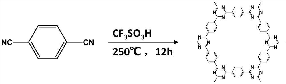
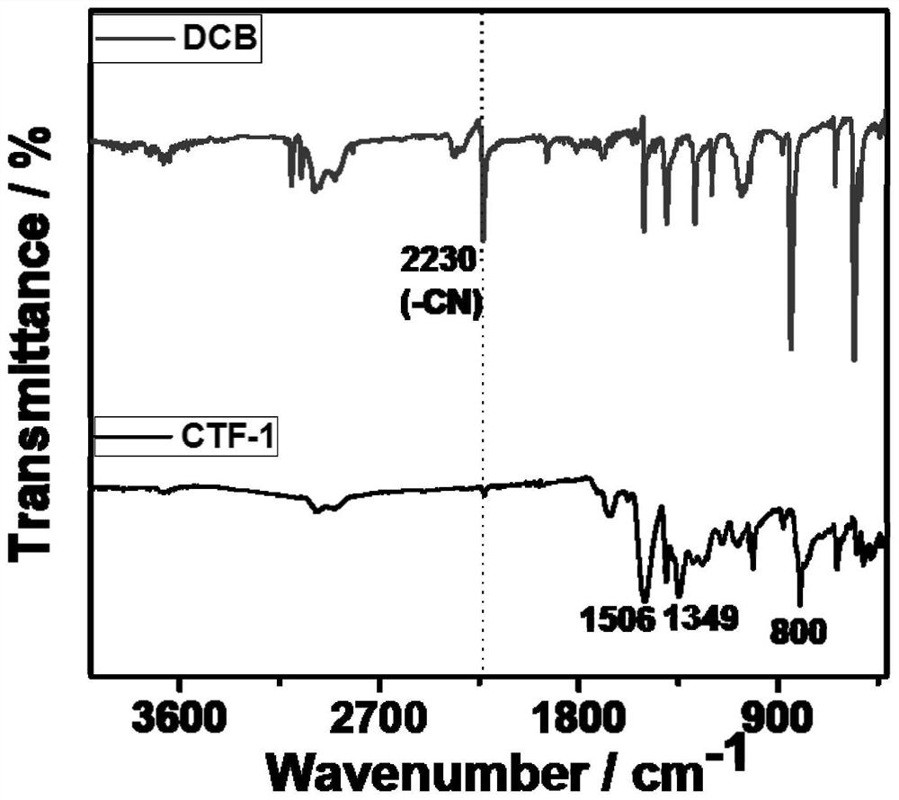
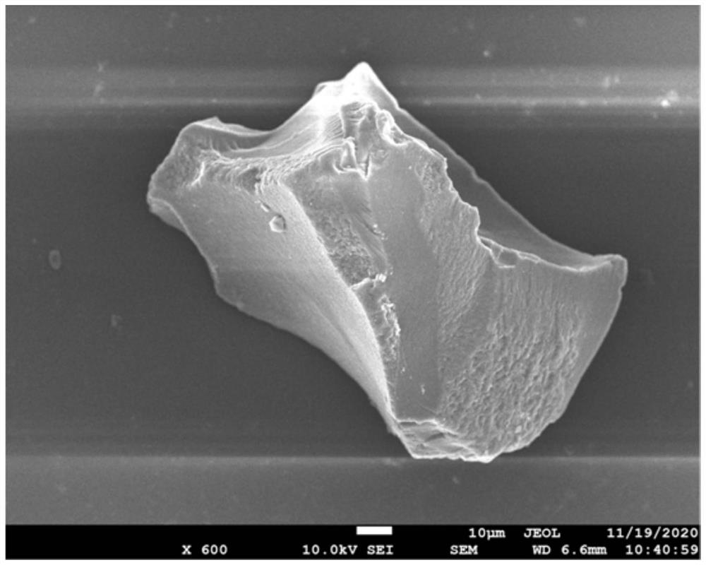
[0056] S1: Terephthalonitrile (2mmol, 0.256g) and trifluoromethanesulfonic acid (CF 3 SO 3 H, 1mmol, 0.15g) is put into the ampoule bottle; The ampoule bottle is carried out freezing, degassing and thawing treatment successively under liquid nitrogen; The ampoule bottle processed through thawing is sealed with flame, and the sealed ampoule bottle is put into Put it into a muffle furnace, heat up from room temperature to 250 °C at a rate of 5 °C / min, and keep it for 12 hours; after completion, cool the ampoule to room temperature and soak it in liquid nitrogen for 10 min; The processed sealed ampoules were opened in a fume hood, the solids were collected, ground into powder, and the powder was washed with water, N,N-dimethylformamide and ethanol in sequence, and the cleaned powder was heated at 100°C Vacuum drying for 12h, ...

Embodiment 2

[0064] This embodiment provides a method for preparing an organic field effect transistor device. The difference between the method of this embodiment and Example 1 is that terephthalonitrile (2mmol) and 1,4-dicyanotetrafluorobenzene (2mmol) ) into an ampoule bottle to prepare a fluorinated donor-acceptor type covalent triazine framework material, and then use the fluorinated donor-acceptor type covalent triazine framework material to prepare an organic field effect transistor device.

[0065] The structure of the organic field effect transistor device prepared according to the method of this embodiment includes Figure 9 The organic semiconductor layer, gate, source and drain are shown.


PUM

PropertyMeasurementUnit
sizeaaaaaaaaaa
strengthaaaaaaaaaa
thicknessaaaaaaaaaa

Abstract

The invention belongs to the field of transistor devices, and discloses an organic field effect transistor device and a preparation method thereof. The preparation method comprises the following steps: preparing a covalent triazine organic framework nanosheet dispersion liquid from a covalent triazine organic framework material through an electrochemical stripping method, and standing; the covalent triazine organic framework nanosheet dispersion liquid is injected to the liquid level of ultrapure water drop by drop, a SiO2/Si substrate penetrates through the interface of the covalent triazine organic framework nanosheet and the ultrapure water, and the SiO2/Si substrate containing the covalent triazine organic framework nanosheet is obtained; and sequentially evaporating a chromium layer and a gold layer on the SiO2/Si substrate containing the triazine covalent organic framework nanosheet by using a vacuum thermal evaporation coating machine to obtain the organic field effect transistor device. The application range of an organic field effect transistor device prepared according to the covalent triazine organic framework material can be widened.

Description

technical field [0001] The invention belongs to the field of transistor devices, and more specifically relates to an organic field effect transistor device and a preparation method thereof. Background technique [0002] Covalent organic frameworks are a class of organic porous polymers with periodicity and crystallinity. Covalent organic framework materials are connected by light elements through covalent bonds, and have low density, high thermal stability and inherent porosity. widespread attention. [0003] Since Yaghi synthesized the first covalent organic framework material in 2005, scientists have developed a large number of organic chemical reactions that can be used to synthesize covalent organic framework materials and synthesized a large number of new covalent organic framework materials. According to the different linking groups, these covalent organic framework materials can be roughly divided into boric anhydride and borate ester series, Schiff base series, imi...

Claims


Application Information

Patent Timeline
Patent Type & Authority Applications(China)
IPC IPC(8): H01L51/05H01L51/30H01L51/10H01L51/40C08G73/06
CPCC08G73/0644H10K71/12H10K71/60H10K85/111H10K10/46H10K10/82
Inventor 乔山林刘海宁李青陈欢李小云颜记朋
Owner HEBEI UNIVERSITY OF SCIENCE AND TECHNOLOGY
Why Eureka
Try Eureka