Two-dimensional material, two-dimensional material alloy and two-dimensional material heterojunction preparation method

A two-dimensional material and heterojunction technology, which is applied in the field of preparation of two-dimensional transition metal chalcogenides, can solve the problems of poor controllability of two-dimensional material growth, poor controllability of two-dimensional material layers, and single crystal quality of two-dimensional materials. To improve controllability and repeatability, realize controllability and high controllability

Pending Publication Date: 2022-04-29
ZHEJIANG UNIV HANGZHOU GLOBAL SCI & TECH INNOVATION CENT
View PDF0 Cites 1 Cited by
  • Summary
  • Abstract
  • Description
  • Claims
  • Application Information

AI Technical Summary

Problems solved by technology

However, this preparation method has more stringent requirements on the quality control of the precursor, and the controllability of the number of layers of the two-dimensional material is poor, and it may lead to residual contamination of the precursor on the substrate.
However, other methods such as chemical solution ratio for 2D material growth may cause other pollution, and the quality of the prepared 2D material single crystal is often poor, and the growth controllability of 2D material is poor.

Method used


Image

  • Two-dimensional material, two-dimensional material alloy and two-dimensional material heterojunction preparation method
  • Two-dimensional material, two-dimensional material alloy and two-dimensional material heterojunction preparation method
  • Two-dimensional material, two-dimensional material alloy and two-dimensional material heterojunction preparation method

Examples


Embodiment 1

[0062] Embodiment 1, the two-dimensional material is single-layer or multi-layer MoS 2 controllable preparation method.

[0063] (1) Preparation of MoO with different thicknesses by thermal evaporation 3 Films as Precursor Films:

[0064] In SiO 2 / Si substrate, that is, the surface layer is coated with 300nm SiO 2 layer of MoO on silicon wafers by thermal evaporation method 3 Thin film, set the thermal evaporation current to about 30A, in the SiO 2 Generate MoO on layer 3 The film deposition rate is Four different thicknesses of MoO can be arbitrarily selected within the range of 1-100nm 3 Thin films to grow monolayer or multilayer MoS 2 , in this example, MoO is obtained respectively 3 MoO with film thickness of 5nm, 30nm, 74nm, 100nm 3 / SiO 2 / Si.

[0065] (2) MoS grown by chemical vapor deposition 2 ;

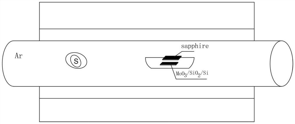
[0066] (2.1) will be coated with MoO 3 thin film MoO 3 / SiO 2 / Si and sapphire substrates are placed in the first evaporation boat, which contains MoO 3...

Embodiment 2

[0072] Embodiment 2, the two-dimensional material is a single layer of WS 2 controllable preparation method.

[0073] (1) Preparation of 30nm WO by thermal evaporation 3 Films as Precursor Films:

[0074] In SiO 2 / Si substrate, that is, the surface layer is coated with 300nm SiO 2 Layers prepared on silicon wafers 3 thin film, set the thermal evaporation current to about 60A, the SiO 2 Generate WO on layer 3 The film deposition rate is Choose to generate WO with a thickness of 30nm 3 , forming WO 3 / SiO 2 / Si to grow monolayer WS 2 .

[0075] (2) Chemical vapor deposition growth WS 2 :

[0076] WO with a film thickness of 30 nm 3 / SiO 2 / Si and sapphire substrates are placed in the first evaporation boat, wherein the MoO 3 The thin film and the sapphire substrate were placed face to face with a distance of 1 mm; the sulfur powder was placed in the second evaporation boat, and the first evaporation boat and the second evaporation boat were respectively placed ...

Embodiment 3

[0077] Embodiment three, the two-dimensional material is Bi 2 S 3 A method for the controllable preparation of nanowires.

[0078] (1) Preparation of 30nm Bi by thermal evaporation 2 o 3 Films as Precursor Films:

[0079] In SiO 2 / Si substrate, that is, the surface layer is coated with 300nm SiO 2 Bi layer prepared on silicon wafer 2 o 3 thin film, set the thermal evaporation current to about 40A, the SiO 2 Generate WO on layer 3 The film deposition rate is Choose Bi 2 o 3 Bi with a film thickness of 30 nm 2 o 3 / SiO 2 / Si to grow Bi 2 S 3 .

[0080] (2) Bi grown by chemical vapor deposition 2 S 3 :

[0081] Bi film with a thickness of 30 nm 2 o 3 / SiO 2 / Si and the sapphire substrate are placed in the first evaporation boat, wherein the Bi 2 o 3 The thin film and the sapphire substrate are placed face to face with a distance of 1mm, the sulfur powder is placed in the second evaporation boat, and the first evaporation boat and the second evaporation ...


PUM

PropertyMeasurementUnit
thicknessaaaaaaaaaa
thicknessaaaaaaaaaa
thicknessaaaaaaaaaa

Abstract

The invention provides a two-dimensional material, a two-dimensional material alloy and a two-dimensional material heterojunction preparation method, and belongs to the technical field of two-dimensional material preparation. A metal film or a metal oxide film is prepared on a silicon wafer through a thermal evaporation coating method to serve as a precursor film, the silicon wafer plated with the precursor film and a substrate are placed in an evaporation boat in a face-to-face mode, the precursor film is vulcanized through a chemical vapor deposition method, and the two-dimensional transition metal chalcogenide grows on the substrate. The two-dimensional material with controllable thickness and size can be obtained by changing the thickness of the precursor film and the face-to-face distance between the silicon wafer and the substrate. The preparation method provided by the invention is universally suitable for growth of two-dimensional materials including two-dimensional transition metal selenium compounds and two-dimensional transition metal tellurium compounds, can be used for preparation of two-dimensional material alloys and heterostructure materials, and is simple in preparation process, high in repeatability and suitable for industrial production. The controllability and the stability of the two-dimensional material in the growth process can be effectively improved.

Description

technical field [0001] The invention belongs to the field of preparation of two-dimensional transition metal chalcogenides, and in particular relates to a method for preparing a two-dimensional material, a two-dimensional material alloy and a two-dimensional material heterojunction. Background technique [0002] Key requirements such as miniaturization and mechanical flexibility of electronic devices have pushed the research field of two-dimensional (2D) materials to the forefront. Atomic-thick 2D crystals cover a very wide range of properties, providing a good material platform to create multifunctional 2D material devices with excellent properties. For example: two-dimensional transition metal dichalcogenides (Transition Metal Dichalcogenides, TMDs), as a representative of 2D materials, have a unique electronic band structure, high mobility, strong spin-orbit coupling and electronic valley structure, in fundamental research and spin It has broad application prospects in e...

Claims


Application Information

Patent Timeline
Patent Type & Authority Applications(China)
IPC IPC(8): C23C28/00C23C14/24C23C14/16C23C14/54C23C16/30C23C16/52C23C14/08H01L21/02
CPCC23C28/322C23C28/34C23C28/345C23C14/24C23C14/16C23C14/542C23C14/083C23C16/305C23C16/52C23C14/086C23C14/08H01L21/02164H01L21/02175H01L21/02236H01L21/02263
Inventor 王佩剑刘影潘宝俊蓝善贵俞滨
Owner ZHEJIANG UNIV HANGZHOU GLOBAL SCI & TECH INNOVATION CENT
Why Eureka
Try Eureka