Wet texturing method for inverted pyramid structure of crystalline silicon

An inverted pyramid and crystalline silicon technology, applied in crystal growth, chemical instruments and methods, semiconductor/solid-state device manufacturing, etc., can solve problems affecting photoelectric conversion efficiency, large inverted pyramid size, large carrier recombination, etc., to achieve improved The effect of photoelectric conversion efficiency, high shape density, and smooth microscopic surface

Pending Publication Date: 2022-06-28
北京师范大学珠海校区
View PDF2 Cites 0 Cited by
  • Summary
  • Abstract
  • Description
  • Claims
  • Application Information

AI Technical Summary

Problems solved by technology

However, this method deposits a large amount of copper, and copper is a deep-level impurity, which will cause large carrier recombination, affect the photoelectric conversion efficiency, and the waste liquid is not friendly to the environment.
However, the above method tends to deposit a large number of copper nanoparticles on the silicon surface during the etching process, and the inverted pyramids that are etched out are large in size and rough in surface, which does not play a good role in reducing the reflectivity.

Method used


Image

  • Wet texturing method for inverted pyramid structure of crystalline silicon

Examples


Embodiment 1

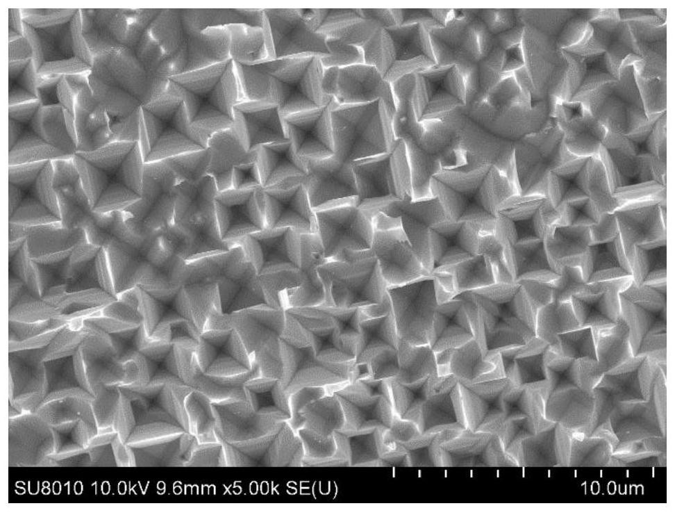
[0018] Put the cleaned single crystal silicon wafer into a polytetrafluoroethylene container containing a mixed solution of 0.5mol / L sodium silicate and 10mol / L hydrofluoric acid for 120 minutes at 80°C, and then etch the silicon wafer with Deionized water wash.

Embodiment 2

[0020] Put the cleaned single crystal silicon wafer into a polytetrafluoroethylene container containing a mixed solution of 0.55mol / L sodium silicate and 10mol / L hydrofluoric acid for 120 minutes at 80°C, and then use the etched silicon wafer with Deionized water wash.

Embodiment 3

[0022] Put the cleaned single crystal silicon wafer into a polytetrafluoroethylene container containing a mixed solution of 0.6mol / L sodium silicate and 10mol / L hydrofluoric acid for 120 minutes at 80°C, and then use the etched silicon wafer with Deionized water wash.


PUM


Abstract

The invention discloses a crystalline silicon inverted pyramid structure wet-method texturing method, and relates to the technical field of new materials and solar energy, in particular to a crystalline silicon inverted pyramid structure wet-method texturing method, which comprises the following steps: putting a crystalline silicon wafer with a clean surface into a container containing a mixed solution of sodium silicate and hydrofluoric acid, reacting for 120-140 minutes at 80 DEG C, filtering, washing, and drying to obtain the crystalline silicon inverted pyramid structure wet-method texturing method. Then, the corroded silicon wafer is put into a deionized water solution to be soaked, and hydrofluoric acid remaining on the surface of the silicon wafer is removed; the invention relates to a crystalline silicon inverted pyramid structure wet texturing method, which comprises the following steps of: putting a crystalline silicon wafer with a clean surface into a container containing a mixed solution of copper chloride, hydrochloric acid, sodium silicate and hydrofluoric acid, and reacting at 80 DEG C for 20 to 40 minutes, so as to corrode a large-area micro-nano inverted pyramid textured surface on the surface of the silicon wafer, and soaking the corroded silicon wafer in an aqua regia solution to remove residual metal on the surface. The preparation process is simple, and the cost is low.

Description

technical field [0001] The invention relates to the technical field of new materials and solar energy, in particular to a wet texturing method of a crystalline silicon inverted pyramid structure. Background technique [0002] Wet chemical etching of crystalline silicon can realize the preparation of various silicon micro-nano structures, and has an important position in the microelectronics, microelectromechanical systems and photovoltaic industries. Etching pyramid arrays on crystalline silicon has a great influence on the photoelectric conversion efficiency of photovoltaic solar cells. However, the current scientific research on solar cells for nearly half a century shows that the conventional preparation method of pyramid array is limited to the preparation of inorganic alkali solution or organic alkali solution (see: Chinese patent CN201310562781.9) or tetramethylammonium hydroxide etching solution (See: Chinese Patent ZL200410017032.9), and the use of acidic hydrofluor...

Claims


Application Information

Patent Timeline
Patent Type & Authority Applications(China)
IPC IPC(8): H01L31/18H01L31/0236H01L21/306C30B33/10
CPCH01L31/1804H01L31/02363H01L21/30608C30B33/10
Inventor 霍晨亮
Owner 北京师范大学珠海校区
Why Eureka
Try Eureka