Method for positioning surface defects of gallium oxide wafer based on photoelectrochemical corrosion process

A photoelectrochemical and gallium oxide technology, applied in chemical instruments and methods, crystal growth, single crystal growth, etc., can solve the problems of locating gallium oxide wafer surface defects, low corrosion rate, long corrosion time, etc., to achieve high-efficiency exposure of defects, Effect of increasing hole concentration and reducing reaction cost

Active Publication Date: 2022-07-08
杭州镓仁半导体有限公司
View PDF12 Cites 0 Cited by
  • Summary
  • Abstract
  • Description
  • Claims
  • Application Information

AI Technical Summary

Problems solved by technology

[0004] The purpose of the present invention is to overcome the problems of low corrosion rate, high reaction temperature and long corrosion time in the traditional method of dislocation identification by corrosion, and provide a method for locating surface defects of gallium oxide wafers based on photoelectrochemical corrosion process

Method used


Image

  • Method for positioning surface defects of gallium oxide wafer based on photoelectrochemical corrosion process
  • Method for positioning surface defects of gallium oxide wafer based on photoelectrochemical corrosion process
  • Method for positioning surface defects of gallium oxide wafer based on photoelectrochemical corrosion process

Examples


Embodiment Construction

[0028] The technical solutions in the embodiments of the present invention will be clearly and completely described below with reference to the accompanying drawings in the embodiments of the present invention. Obviously, the described embodiments are only a part of the embodiments of the present invention, but not all of the embodiments. Based on the embodiments of the present invention, all other embodiments obtained by those of ordinary skill in the art without creative efforts shall fall within the protection scope of the present invention.

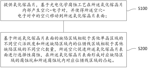
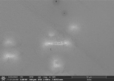
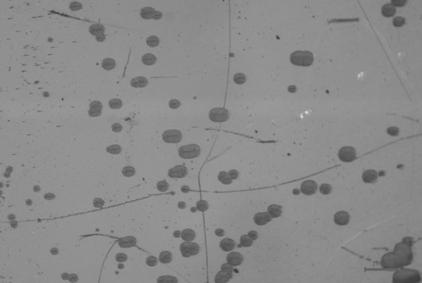
[0029] see figure 1 , this embodiment provides a technical solution: a method for locating surface defects of a gallium oxide wafer based on a photoelectrochemical etching process, comprising the following steps:

[0030] Step S100, providing a gallium oxide wafer, generating hole-electron pairs inside the gallium oxide wafer based on a photoelectrochemical etching process, and making the holes in the hole-electron pair move to the su...


PUM


Abstract

The invention relates to the technical field of semiconductor processing, and discloses a method for positioning surface defects of a gallium oxide wafer based on a photoelectrochemical corrosion process, and the method comprises the steps: generating a hole-electron pair in the gallium oxide wafer based on the photoelectrochemical corrosion process, and enabling a hole in the hole-electron pair to move to the surface of the gallium oxide wafer along with the bending of an energy band; based on different hole activeness of a defect region on the surface of the gallium oxide wafer compared with other single crystal regions, different numbers of holes caused by hole-electron pair recombination easily occurring in a dislocation line region in the defect region and position distribution of dislocation lines in an etching pit region; selectively-corroded corrosion pits and protrusions corresponding to dislocation line areas in the corrosion pits are formed on the surface of the gallium oxide; the method greatly improves the corrosion rate, has the advantage of high-efficiency dislocation exposure, greatly reduces the reaction risk, reduces the reaction cost, and has industrial development prospects.

Description

technical field [0001] The invention relates to the technical field of semiconductor processing, in particular to a method for locating surface defects of gallium oxide wafers based on a photoelectrochemical etching process. Background technique [0002] As a transparent oxide semiconductor material, gallium oxide single crystal has attracted worldwide attention due to its ultra-wide band gap (4.9 eV). MV / cm, much higher than silicon (1.1 eV, 0.3 MV / cm), gallium arsenide (1.4 eV, 0.4 MV / cm), silicon carbide (3.3 eV, 2.5 MV / cm), and gallium nitride (3.4 eV, 3.3 MV / cm) and other semiconductor materials; at the same time, gallium oxide also has the advantages of unique ultraviolet transmission characteristics, low energy consumption, high thermal stability and chemical stability, etc. Preferred semiconductor material for blind UV photodetectors and UV transparent conductive electrodes. [0003] In order to make full use of the advantages of gallium oxide semiconductors to pre...

Claims


Application Information

Patent Timeline
IPC IPC(8): C25F3/12C25F3/14C30B29/16C30B33/10G01N1/32
CPCC25F3/12C25F3/14C30B29/16C30B33/10G01N1/32Y02P70/50
Inventor 张辉金竹刘莹莹杨冉夏宁杨德仁
Owner 杭州镓仁半导体有限公司
Why Eureka
Try Eureka