Inorganic perovskite solar cell based on substituted hydrazide and preparation method thereof
A technology of solar cells and inorganic calcium, applied in circuits, electrical components, photovoltaic power generation, etc., can solve the problems of perovskite film defects, poor optoelectronic properties, and non-radiative recombination.
- Summary
- Abstract
- Description
- Claims
- Application Information
AI Technical Summary
Problems solved by technology
Method used
Image
Examples
Embodiment 1
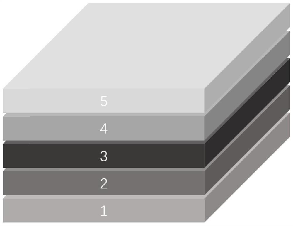
[0071] First, clean the conductive glass substrate: use a mixture of ultrapure water and glass cleaning agent v / v=100:1 to clean the conductive glass FTO substrate for 30 minutes, and then change the ultrapure water for 3 times, each cleaning for 30 minutes, with air The compressor will dry the cleaned conductive glass FTO substrate for use.
[0072] Second, prepare the electron transport layer on the prepared conductive glass FTO substrate: UV-ozone treatment of the FTO substrate for 10-15min, and then TiCl 4 Aqueous solution to deposit a layer of TiO on FTO substrate by water bath deposition method 2 As the electron transport layer, the deposition temperature was 70 °C and the deposition time was 60 min.
[0073] Third, prepare the perovskite precursor solution: prepare CsPbI with a concentration of 0.745M 3 Perovskite precursor solution. 0.4387g HPbI 3 and 0.1935g CsI were dissolved in a mixed solution of DMF and DMSO with a volume ratio of 17:3 to prepare inorganic CsP...
Embodiment 2
[0099] In this example, the prepared CsPbI 3 Perovskite precursor solution, the addition content of BH is 1.5%. Other steps are the same as in Example 1. In this example, the 1.5% BH-added perovskite cell device has an open circuit voltage of 1.200 V and a photoelectric conversion efficiency of 19.68%.
Embodiment 3
[0101] In this example, the prepared CsPbI 3 Perovskite precursor solution, the addition content of BH is 6%. Other steps are the same as in Example 1. In this example, the 6% BH-added perovskite cell device has an open circuit voltage of 1.196 V and a photoelectric conversion efficiency of 19.30%.
PUM
| Property | Measurement | Unit |
|---|---|---|
| Thickness | aaaaa | aaaaa |
| Thickness | aaaaa | aaaaa |
| Thickness | aaaaa | aaaaa |
Abstract
Description
Claims
Application Information


