
Perovskite light emitting diode containing modification layer and evaporation preparation method thereof

A technology of light-emitting diodes and perovskites, which is applied in the field of preparation of perovskite light-emitting diodes, can solve the problems of many film defects, poor appearance quality of perovskite light-emitting layers, and poor performance of light-emitting diodes, so as to increase device performance, Improving carrier transport efficiency and improving the effect of interface barrier

Pending Publication Date: 2022-07-08
HEBEI UNIV OF TECH
View PDF0 Cites 0 Cited by
  • Summary
  • Abstract
  • Description
  • Claims
  • Application Information

AI Technical Summary

Problems solved by technology

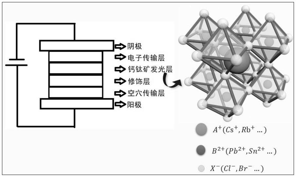
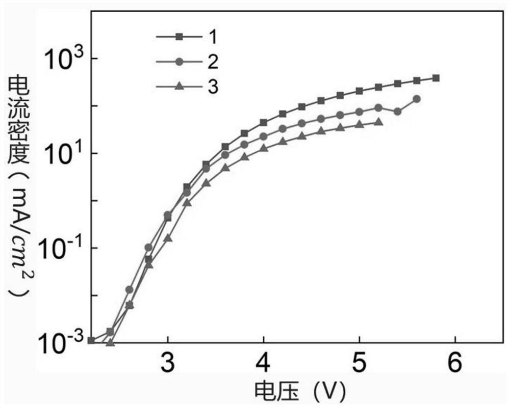
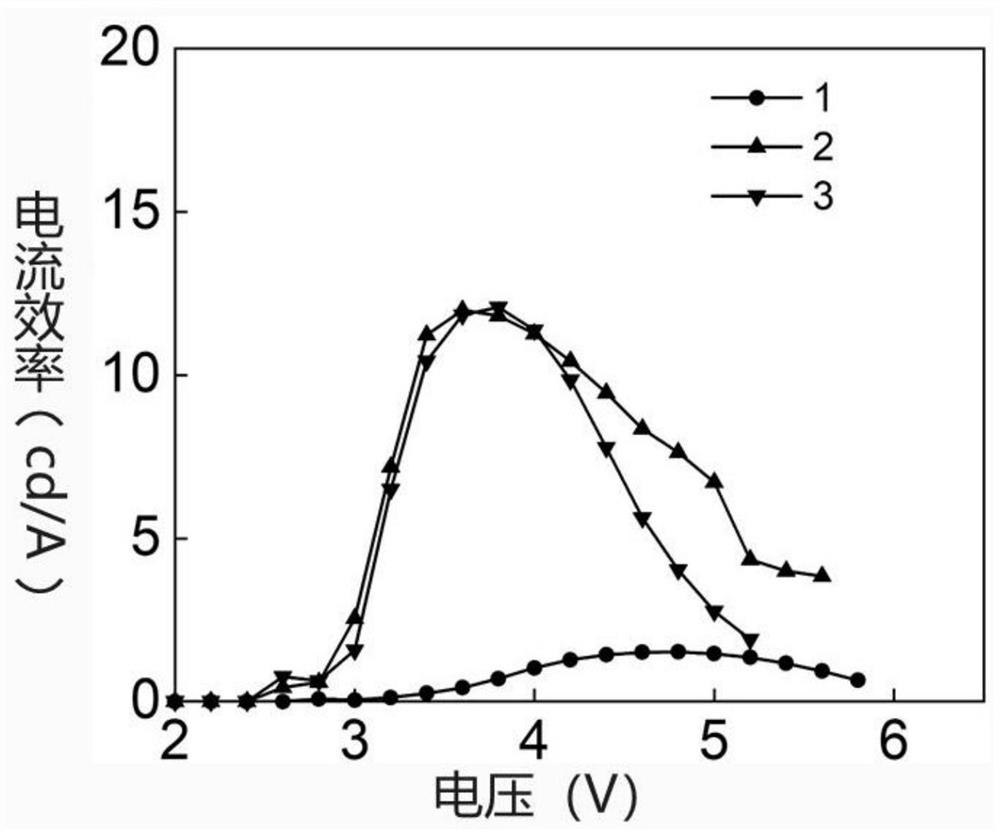
[0004] The purpose of the present invention is to solve the technical problems that the perovskite light-emitting layer has poor morphology quality and many film defects in the preparation of perovskite light-emitting diodes in the prior art, resulting in poor performance of light-emitting diodes, and to provide a method for improving the perovskite light-emitting diode. The method of diode performance, this method is between the hole transport layer and the vapor-deposited perovskite light-emitting layer to make a modified layer of amino acid compound material. The carboxyl and amino groups in amino acids can play a great role, because the molecules Coulomb interaction, so that the functional groups in the positive and negative ions and amino acids can be combined, such as -COOH and the excess Pb in the perovskite light-emitting layer 2+ ion, -NH 2 with Br - Interactions are formed between ions, thereby passivating the anion and cation defects on the surface, thereby suppressing the non-radiative recombination defects of the perovskite film, improving the fluorescence quantum efficiency of the light-emitting layer, and further improving the performance of the device. At the same time, the introduction of the interface layer can improve The interface barrier can improve the injection efficiency of carriers to the light-emitting layer, thereby improving the electroluminescence performance of the device such as brightness, current efficiency and external quantum efficiency, etc.

Method used


Image

  • Perovskite light emitting diode containing modification layer and evaporation preparation method thereof
  • Perovskite light emitting diode containing modification layer and evaporation preparation method thereof
  • Perovskite light emitting diode containing modification layer and evaporation preparation method thereof

Examples


Embodiment 1

[0071] The preparation method of the second perovskite light-emitting diode comprises the following steps:

[0072] ①The preparation process of 4-aminobutyric acid is to stir 100mg of drug powder and 1ml of deionized water evenly. Take 0.1 ml of 4-aminobutyric acid solution and 1 ml of PEDOT:PSS (the volume ratio of the two is 1:10), mix and stir, and the hole transport layer includes poly(3,4-ethylenedioxythiophene)-poly( styrene sulfonate) (PEDOT:PSS). The amino acid solution can be doped with water-soluble PEDOT:PSS solution and then spin-coated. Mix 100 microliters of 4-aminobutyric acid with a concentration of 100 mg / ml and 1000 microliters of PEDOT:PSS to obtain a mixed solution;

[0073] ②The ultrasonic-treated glass substrate (20*20mm) with a transparent anode layer (185nm thick, single ITO is 4*20mm), i.e. indium tin oxide (ITO), was placed on the spin coater after UV ozone treatment, and 0.05ml of The mixed solution obtained in the previous step was evenly coated ...

Embodiment 2

[0079] The preparation method of the second perovskite light-emitting diode comprises the following steps:

[0080] ①The preparation process of 4-aminobutyric acid is to mix 50mg of drug powder and 1ml of deionized water evenly. 0.1 ml of 4-aminobutyric acid solution and 1 ml of PEDOT:PSS were mixed and stirred, and the hole transport layer included poly(3,4-ethylenedioxythiophene)-poly(styrene sulfonate) (PEDOT:PSS). The amino acid solution can be doped with water-soluble PEDOT:PSS solution and then spin-coated. Mix 100 microliters of 50 mg / ml 4-aminobutyric acid with 1000 microliters of PEDOT:PSS to obtain a mixed solution

[0081] ② Put the ultrasonically treated glass substrate (20*20mm) with a transparent anode layer (185nm thick, a single ITO is 4*20mm), that is, indium tin oxide (ITO), on the spin coater after UV ozone treatment, take 0.05ml The mixed solution obtained in the previous step was evenly coated on the entire film, and was spin-coated at a speed of 6000 rp...

Embodiment 3

[0087] The preparation method of the first perovskite light-emitting diode comprises the following steps:

[0088] ①The preparation process of glycine solution is to mix 50mg of drug powder and 1ml of deionized water evenly.

[0089] ②The ultrasonic-treated glass substrate (20*20mm) with a transparent anode layer (185nm thick, a single ITO is 4*20mm), that is, indium tin oxide (ITO), was placed on the spin coater after UV ozone treatment, and passed through 0.22 micron The filter uniformly coats the entire film with PEDOT:PSS, spin-coating at 6000 rpm for 30 s through a spin coater, and annealing at 140°C for 10 minutes to form a hole transport layer on the anode.

[0090] ③Place the annealed substrate with the hole transport layer on the spin coater, take 0.1ml of 50mg / ml glycine with a pipette and spin-coat on the substrate, and spin the spin coater at a speed of 8000 rpm for 30s , and the interface modification layer was formed after high temperature annealing at 100°C for...


PUM

PropertyMeasurementUnit
Thicknessaaaaaaaaaa
Thicknessaaaaaaaaaa

Abstract

The invention relates to a perovskite light-emitting diode containing a modification layer and an evaporation preparation method of the perovskite light-emitting diode. According to the first type, a metal cathode, an electron transport layer, a perovskite light-emitting layer, an interface modification layer, a hole transport layer and ITO conductive glass are sequentially arranged from top to bottom; or, according to the second type, the metal cathode, the electron transport layer, the perovskite light-emitting layer, the interface modification / hole transport mixed layer and the ITO conductive glass are sequentially arranged from top to bottom; and the interface modification layer is an amino acid (CH2) nCHNH2COOH compound. The interface layer is added between the hole transport layer and the perovskite layer of the perovskite light-emitting diode, so that the interface barrier is improved, the interface defect passivation effect is achieved, the carrier transport efficiency is improved, the electroluminescence and photoluminescence efficiency is enhanced, and the device brightness, the current efficiency and other performance are improved.

Description

technical field [0001] The invention relates to the technical field of light-emitting diodes, in particular to a preparation method of a perovskite light-emitting diode that can improve performance. Background technique [0002] Lead-halide perovskites, as the light-emitting layer of LEDs, have the following advantages: (1) The luminescence peak position can be adjusted in the visible light or even near-infrared light range through component design; (2) It has a high defect tolerance and can obtain high Fluorescence yield, luminescence purity and ultra-wide luminescence color gamut; (3) With bipolar charge transport capability, the carrier mobility is higher, and the device can obtain higher brightness; (4) Perovskite The preparation cost of LED is low, including raw materials, equipment and preparation methods all meet the requirements of low cost. The molecular formula of the all-inorganic perovskite material is CsPbX 3 , where Cs is cesium, Pb is lead, and X is one of i...

Claims


Application Information

Patent Timeline
IPC IPC(8): H01L51/50H01L51/52H01L51/54H01L51/56C23C14/06C23C14/24
CPCC23C14/24C23C14/0694H10K85/141H10K85/1135H10K85/60H10K50/00H10K50/84H10K71/00Y02E10/549
Inventor 宋丽续浩赵立昂胡永生
Owner HEBEI UNIV OF TECH
Learn More