Photo-electric equipment and batch spherical semiconductor grain producing equipment
A technology of optoelectronic equipment and semiconductors, which is applied in semiconductor devices, semiconductor/solid-state device manufacturing, crystal growth, etc., and can solve problems such as poor cost reduction
- Summary
- Abstract
- Description
- Claims
- Application Information
AI Technical Summary
Problems solved by technology
Method used
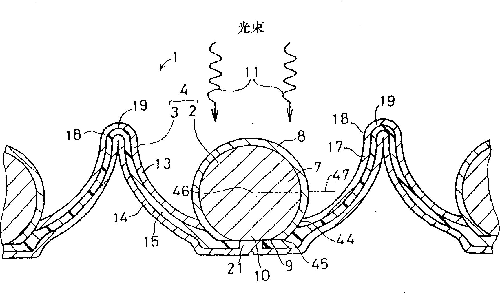
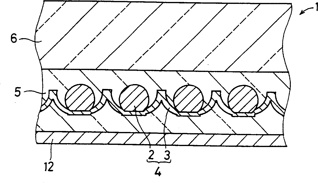
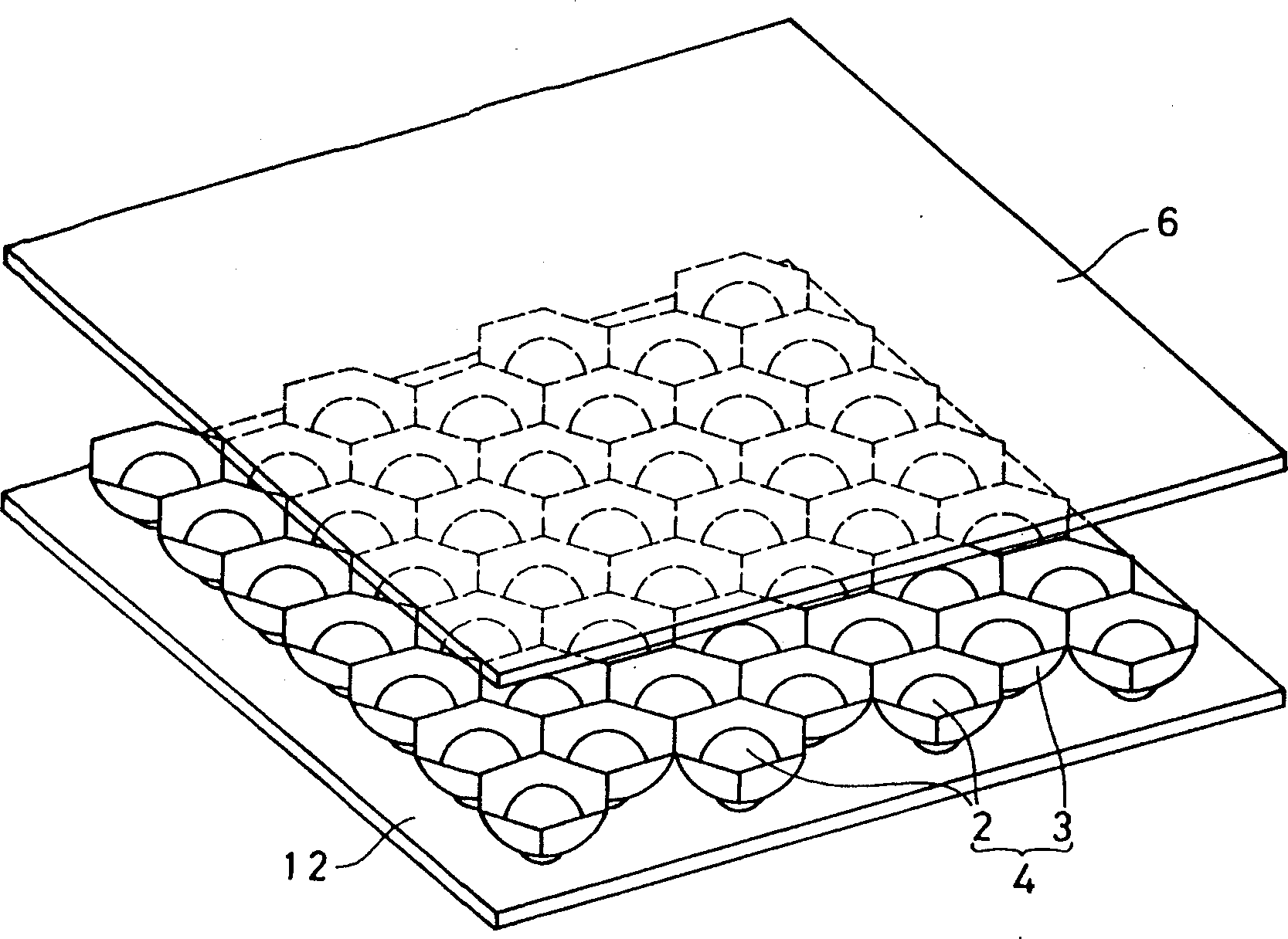
Image

Examples
example 1
[0213] About 1.5 ml of silicon material was added to a graphite crucible. The graphite crucible has an outer diameter of 20 mm, an outer length of 40 mm, its volume is represented by an inner diameter of 10 mm and a length of 35 mm, and is accommodated in a ceramic airtight and thermally insulated container with a nozzle at one end of the container having an inner diameter of 1 mm and a length of 5 mm. Immediately before particle production, 4.6kW of high-frequency induction power was applied for about 20 minutes to stabilize particle production conditions such as temperature. Particle formation was started by applying a nitrogen pressure of about 300 Pa, resulting in silicon spheres having an average diameter of about 1 mm. In order to reduce the degree of reaction between silicon and graphite and the degree of combustion of graphite due to the presence of oxygen, a nitrogen pressure of about 100 Pa is maintained in the system where the flow rate becomes zero at the beginning...
example 2
[0215] About 1.5 ml of silicon material was added to a graphite crucible. The graphite crucible has an outer diameter of 20 mm, an outer length of 40 mm, its volume is represented by an inner diameter of 10 mm and a length of 30 mm, and is accommodated in a ceramic airtight and heat-insulated container with a nozzle of an inner diameter of 1 mm and a length of 10 mm at one end of the container. Immediately before particle production, 4.6kW of high-frequency induction power was applied for about 15 minutes to stabilize particle production conditions such as temperature. Particle formation was started by applying a nitrogen pressure of about 500 Pa, resulting in silicon spheres having an average diameter of about 1 mm. In order to reduce the degree of reaction between silicon and graphite and the degree of combustion of graphite due to the presence of oxygen, a nitrogen pressure of about 100 Pa is maintained in the system where the flow rate becomes zero at the beginning of appl...
example 3
[0217] About 1.2 ml of silicon material was added to a graphite crucible. The graphite crucible has an outer diameter of 20 mm, an outer length of 40 mm, its volume is represented by an inner diameter of 10 mm and a length of 25 mm, and is accommodated in a ceramic airtight and heat-insulated container with a nozzle of an inner diameter of 1 mm and a length of 10 mm at one end of the container. Immediately before particle production, a high-frequency induction power of 3.6kW was applied for about 20 minutes to stabilize particle production conditions such as temperature. Particle formation was started by applying a nitrogen pressure of about 300 Pa, resulting in silicon spheres having an average diameter of about 1 mm. In order to reduce the degree of reaction between silicon and graphite and the degree of combustion of graphite due to the presence of oxygen, a nitrogen pressure of about 100 Pa is maintained in the system where the flow rate becomes zero at the beginning of ap...
PUM
 Abstract
Description
Claims
Application Information