Laser-inducing preparation of size-controllable high-density nano silicon quanta array of points

A nano-silicon quantum dot, laser-induced technology, applied in nanotechnology, nanotechnology, nanostructure manufacturing, etc., can solve the problems of high cost, achieve the effect of reducing interface state density, strong controllability, and avoiding high temperature treatment process

Inactive Publication Date: 2003-08-27
NANJING UNIV
View PDF0 Cites 8 Cited by
  • Summary
  • Abstract
  • Description
  • Claims
  • Application Information

AI Technical Summary

Problems solved by technology

[0004] The purpose of the present invention is exactly to the requirement of above three respects, proposes the new technology principle of preparation size controllable nano-silicon quantum dot, designs and provides a kind of new technical method in experiment simultaneously, utilizes this method not only with current microelectronic technology Compatible with the technology and avoiding the use of expensive ultra-fine processing technology, while obtaining high-density nano-silicon quantum dots with controllable size, it can also effectively passivate the surface of the nano-crystal grains to reduce the density of defect states, so it can show Quantum effects due to size changes

Method used


Image

  • Laser-inducing preparation of size-controllable high-density nano silicon quanta array of points
  • Laser-inducing preparation of size-controllable high-density nano silicon quanta array of points
  • Laser-inducing preparation of size-controllable high-density nano silicon quanta array of points

Examples


Embodiment Construction

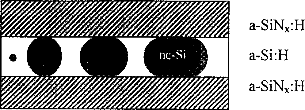
[0026] 1. a-Si:H / a-SiN x : Preparation of H multilayer modulation structure

[0027] Using computer-controlled plasma-enhanced vapor deposition (PECVD) technology, using silane (SiH 4 ), ammonia (NH 3 ) and argon (Ar) as the reaction gas source; depositing a-Si: H / a-SiN on single crystal silicon wafers and quartz or optical glass substrates x : H three-layer or multi-layer modulation structure. Concrete process conditions during preparation are as follows:

[0028] Power source frequency: 13.56MHz

[0029] Power density during deposition: 0.2-0.3W / cm 2

[0030] Reaction chamber pressure: 33-40Pa

[0031] Substrate temperature: 250°C

[0032] When depositing the amorphous silicon (a-Si:H) sublayer, the SiH 4 +Ar is produced by glow decomposition reaction, where SiH 4 The flow rate is 8sccm (standard cubic centimeter per minute), and its deposition rate is 0.10nm / s; the amorphous silicon nitride (a-SiN:H) subl...


PUM

PropertyMeasurementUnit
wavelengthaaaaaaaaaa
diameteraaaaaaaaaa
thicknessaaaaaaaaaa

Abstract

The method for preparing size-controllable high-density nano silicon quantum point array by laser induction includes: firstly, preparing multilayer modulated structure; using plasma reinforced chemical vapor-phase sedimentation techinque to prepare amorphous silicon orgermaium / amorphous silicon nitride or silicon dioxide single-layer or multilayer modulated structure, in which a-Si:H sublayer thickness is basically in accord with laser crystallized desired quantum point size; then using laser to induce crystallization; the substrate temp. is 150-250 deg.C.

Description

1. Technical field: [0001] The present invention proposes a new method for preparing a size-controllable high-density nano-silicon quantum dot array from two aspects of technical principle and implementation process, especially the preparation of a size-controllable high-density nano-silicon quantum dot array based on the principle of laser-induced restricted crystallization The array method, that is, the single-layer or multi-layer modulation structure of amorphous silicon or germanium / amorphous silicon nitride or silicon dioxide is prepared by plasma-enhanced chemical vapor deposition technology, which is a new generation of nano-electronics and nano-optoelectronics Key technologies in high-tech fields such as devices. 2. Background technology: [0002] Semiconductor monocrystalline silicon material is the backbone material of the current microelectronics industry, and has an irreplaceable position for other materials. However, can silicon materials continue to play an im...

Claims


Application Information

Patent Timeline
Patent Type & Authority Applications(China)
IPC IPC(8): B82B3/00C30B29/60
CPCB82Y30/00C30B29/605
Inventor 黄信凡陈坤基李伟徐骏冯端王明湘姜建功施伟华
Owner NANJING UNIV
Why Eureka
Try Eureka