Method for making dimethyl silicone polymer micro flow control chip composite type optical cured resin die arrangement

A polydimethylsiloxane and microfluidic chip technology, applied in the field of micro-manufacturing, can solve the problems of pattern cracks, many processes, long time, etc., and achieves the effect of clean and clear structure outline and improved development speed and quality.

Inactive Publication Date: 2005-06-01
XI AN JIAOTONG UNIV
View PDF0 Cites 51 Cited by
  • Summary
  • Abstract
  • Description
  • Claims
  • Application Information

AI Technical Summary

Problems solved by technology

However, the production process of this kind of photoresist mold takes a long time and has many processes. Before exposure, the photoresist needs to

Method used


Image

  • Method for making dimethyl silicone polymer micro flow control chip composite type optical cured resin die arrangement
  • Method for making dimethyl silicone polymer micro flow control chip composite type optical cured resin die arrangement

Examples


Embodiment Construction

[0044] According to the above technical solution, the present invention provides a specific embodiment. It should be noted that the present invention is not limited to this embodiment, and the parameter transformation performed within the scope of the above technical solution belongs to the protection scope of the present invention.

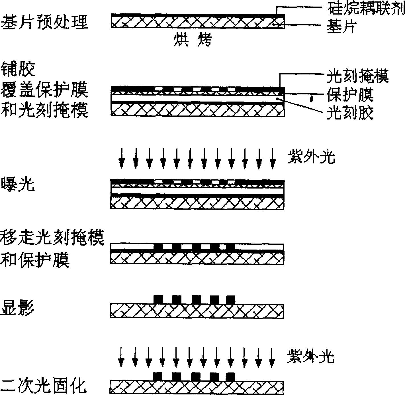
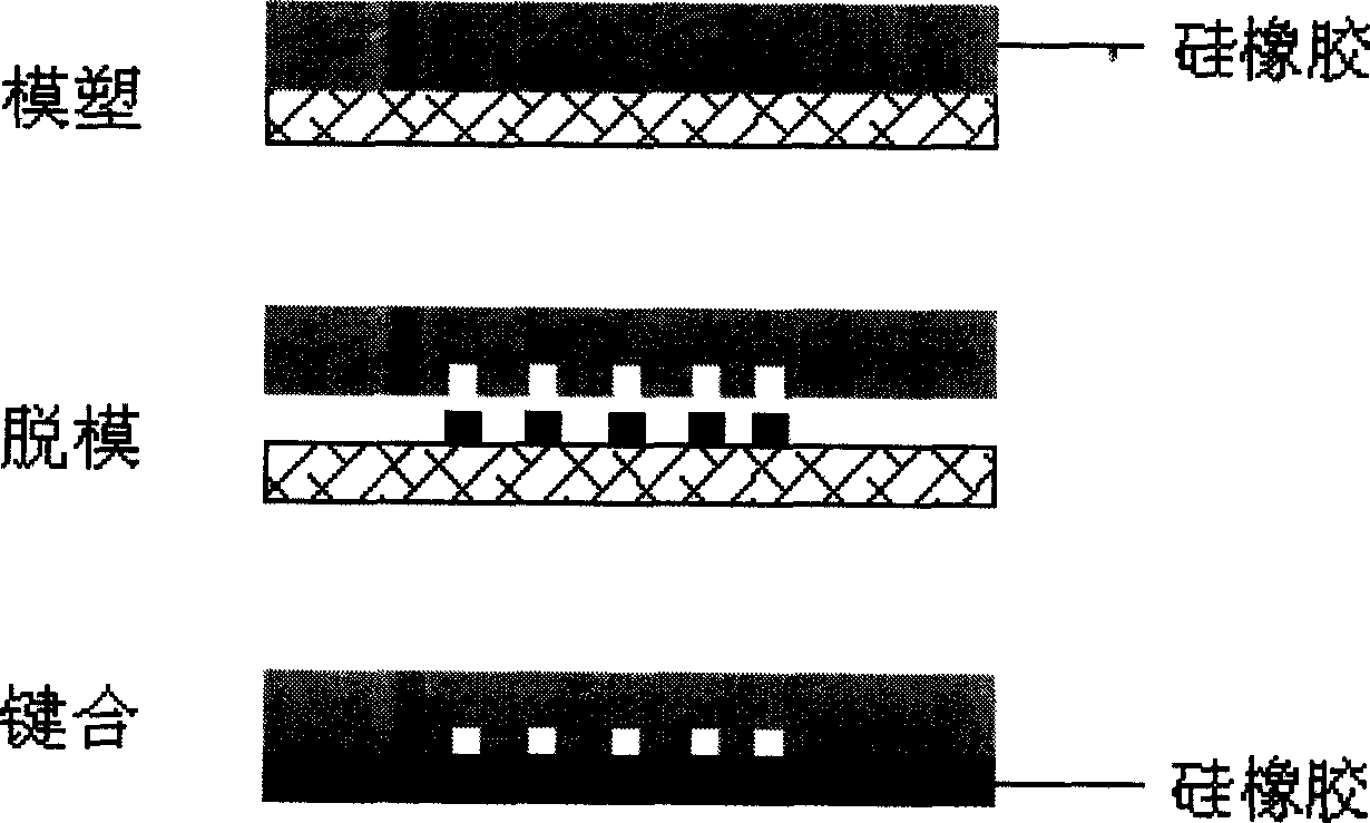
[0045] (1) Mold making

[0046] 1. Substrate pretreatment

[0047] Using quartz or glass as the substrate material, the substrate is pretreated to increase the bonding force between the photoresist and the substrate. The pretreatment method is to take a small amount of silane coupling agent (commercially available), evenly coat the substrate, put it into an oven, and bake at 120° C. for 40 minutes.

[0048] 2. Laying glue

[0049] A plastic sheet is pasted around the substrate to form a cavity, and after the photoresist is injected into the cavity, it is scraped off with a scraper.

[0050] 3. Exposure

[0051] Cover a layer of F46 protective...


PUM


Abstract

The present invention discloses the making process of composite photocuring resin mold for preparing microfluid controlling chip of polydimethyl siloxane. The present invention adopts liquid photoresist of photosensitive epoxy resin as micro mold material, quartz glass as substrate, silane coupler coating on the substrate to increase the binding force between the mold structure and the substrate, plastic film of different thickness adhered around the substrate to control the thickness of photoresist, photoetching mask of photosensitive film from laser photoset, common ultraviolet lamp or ultraviolet laser as exposure light source, F46 film as exposure protecting film, absolute alcohol as developer, vibration for clear development contour and secondary photocuring after development to raise structure strength and structure-substrate binding force. The mold is used in copying microfluid control chip, biochip, soft mold for impression etching, etc.

Description

technical field [0001] The invention belongs to the technical field of micro-manufacturing, and in particular relates to a method for manufacturing a polydimethylsiloxane microfluidic chip replica photocurable resin mold. Background technique [0002] The microfluidic chip is mainly used in analytical chemistry. It integrates the functions of the entire laboratory, including sampling, dilution, reagent addition, reaction, separation, detection, etc., on a tiny chip characterized by a micropipeline network. Due to the high heat conduction and mass transfer rate in the micron-scale channel, the analysis speed is greatly improved, and the consumption of precious samples is greatly reduced, so the analysis system is developing in the direction of miniaturization, and the key to making a microfluidic chip is its microfabrication technology. Traditional micromachining technology mainly uses silicon wafers or glass as structural materials to make microfluidic channels. Due to prob...

Claims


Application Information

Patent Timeline
IPC IPC(8): G03F7/20
Inventor 段玉岗徐书洁丁玉成卢秉恒
Owner XI AN JIAOTONG UNIV
Why Eureka
Try Eureka