

La1-xAxMnO3 thin films and heterojunction materials grown denotatively on the silicon chip and preparing method
A lanthanum manganate thin film and epitaxial growth technology is applied in the field of epitaxial growth heterojunction thin film materials, and can solve the problems of doping lanthanum manganate epitaxial growth and the like
- Summary
- Abstract
- Description
- Claims
- Application Information
AI Technical Summary
Problems solved by technology
Method used
Image

Examples
Embodiment 1
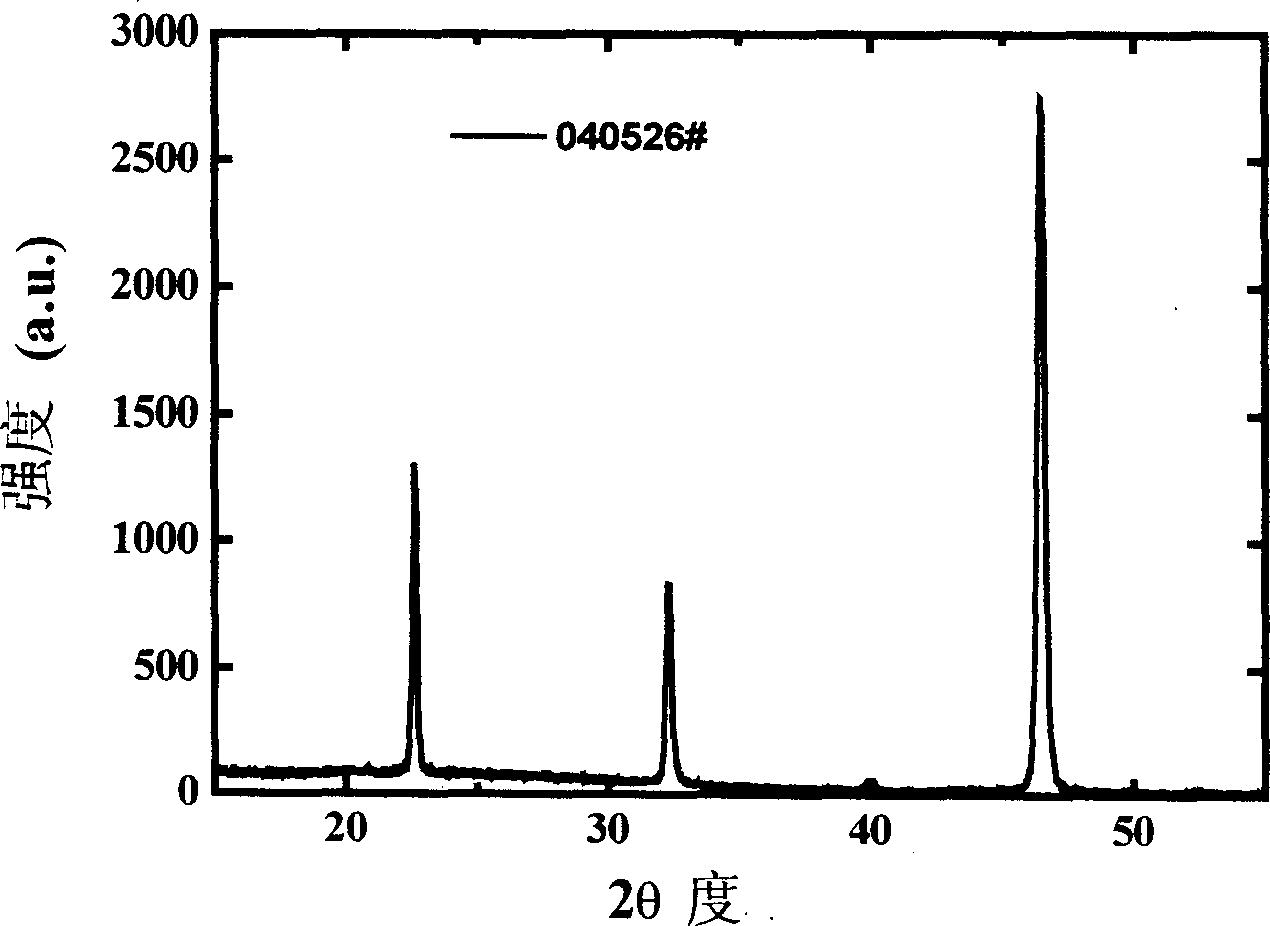
[0042] Use conventional laser molecular beam epitaxy equipment to epitaxially grow 500nm thick La on n-type silicon wafers 0.7 Sr 0.3 MnO 3 film.
[0043] The La 0.7 Sr 0.3 MnO 3 The film itself is a magnetic functional material with magnetoresistance properties, and the La 0.7 Sr 0.3 MnO 3 The heterojunction composed of / Si is a p-n thin film heterojunction material with good magnetic function characteristics.
[0044] La in this example 0.7 Sr 0.3 MnO 3 The specific preparation process of thin film heterojunction materials is:
[0045] 1. Choose a no-clean 2-inch single-side polished n-type single crystal Si substrate;
[0046] 2. Use high-temperature sintered p-type La 0.7 Sr 0.3 MnO 3 target;
[0047] 3. After rinsing in 1% hydrofluoric acid washing solution for 10 seconds, directly put the silicon wafer into the epitaxial chamber;
[0048] 4. Vacuum the epitaxial chamber to 2×10 -5 Pa, using an excimer laser with an output energy of 250 mJ, sputtering ~5...
Embodiment 2
[0053] The La of 800nm is prepared by the method for embodiment 1 0.8 Sr 0.2 MnO 3 Film and La 0.8 Sr 0.2 MnO 3 / Si p-p junction thin film heterojunction materials.
[0054] Use p-type silicon wafers as substrates, and use p-type high-temperature sintered La 0.8 Sr 0.2 MnO 3 Target, other conditions are the same as in Example 1, the different conditions: 3 × 10 people in the epitaxial chamber during epitaxial growth -1 Pa reactive oxygen species to prepare 800nm La 0.8 Sr 0.2 MnO 3 Film and La 0.8 Sr 0.2 MnO 3 / Si p-p thin film heterojunction materials.
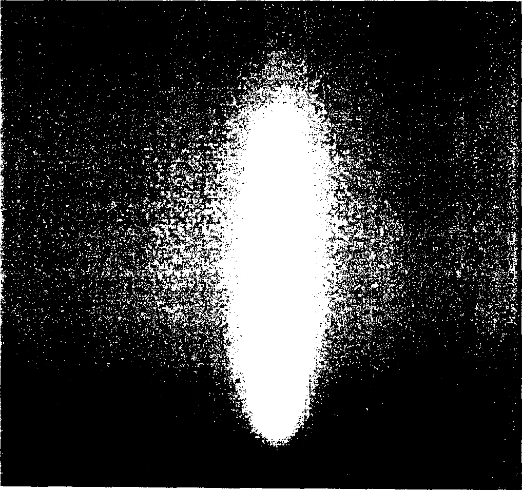
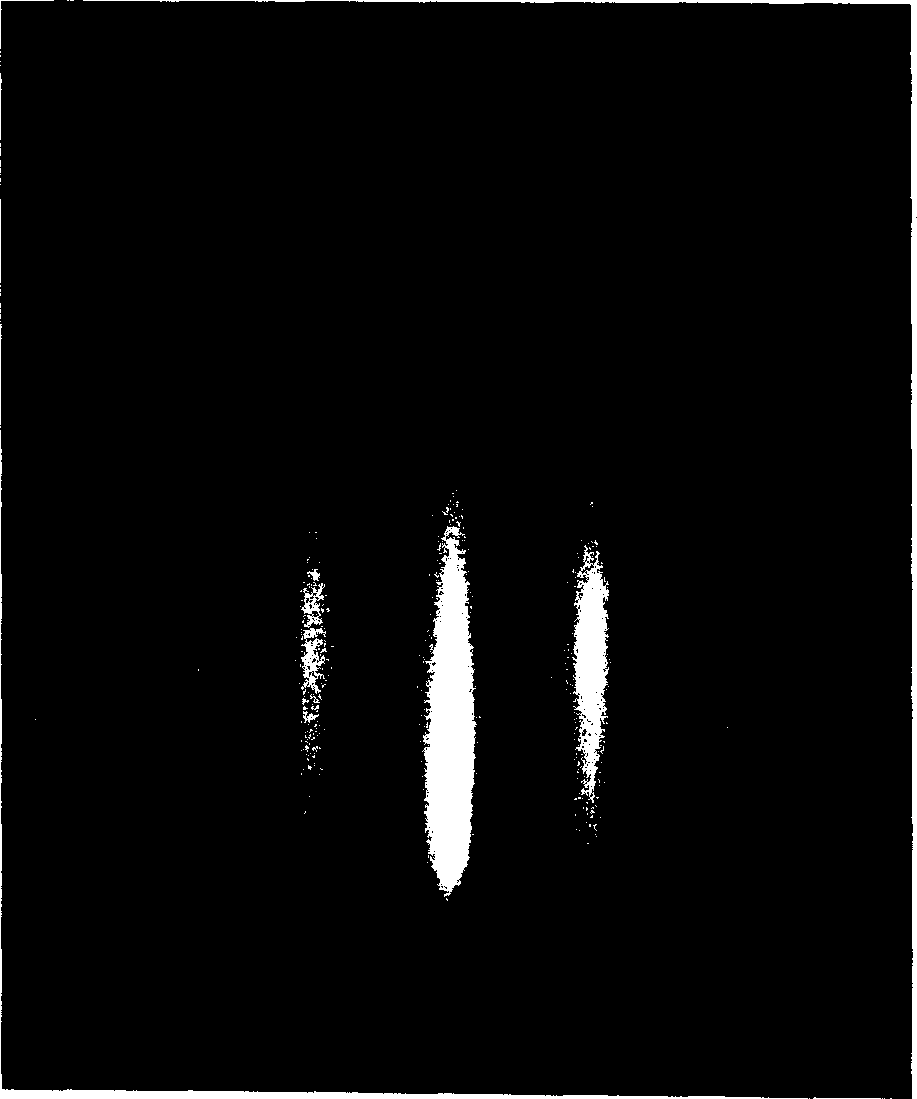
[0055] figure 2 For the epitaxial growth of 400nm thick La on p-type Si substrate 0.8 Sr 0.2 MnO 3 RHEED diffraction fringes of the film. Sharp and clear RHEED diffraction fringes, illustrating the epitaxially grown La on p-type Si substrate 0.8 Sr 0.2 MnO 3 The film not only has good crystallinity, but also has a smooth surface.
Embodiment 3
[0057] According to the method of embodiment 1, the preparation takes n-type single crystal Si as the substrate, and the La after epitaxial growth 800nm 0.9 Ca 0.1 MnO 3Film and La 0.9 Ca 0.1 MnO 3 / Si p-n heterojunction materials.
[0058] with p-type La 0.9 Ca 0.1 MnO 3 Target material, pass people 3×10 in the epitaxial chamber during epitaxial growth -1 Pa reactive oxygen species to prepare 800nm La 0.9 Ca 0.1 MnO 3 Film and La 0.9 Ca 0.1 MnO 3 / Si p-n junction.
PUM
 Abstract
Description
Claims
Application Information