
Method for making laser-electric absorption modulator-spot-size converter single chip integration

A technology of electro-absorption modulator and speckle converter, which is applied to lasers, laser components, semiconductor lasers, etc., can solve the problems of modulation bandwidth limitation, complex process, poor crystal quality at the joint between modulator and speckle converter

Inactive Publication Date: 2006-06-21
INST OF SEMICONDUCTORS - CHINESE ACAD OF SCI
View PDF0 Cites 17 Cited by
  • Summary
  • Abstract
  • Description
  • Claims
  • Application Information

AI Technical Summary

Problems solved by technology

The three mode spot converters have their own advantages and disadvantages: the thickness of the vertical wedge-shaped waveguide changes gradually from the active area to the output end face
[0008] (1) Most of the lasers and modulators use buried structures, many epitaxy times, complex processes, and low device reliability
[0009] (2) The speckle converter adopts vertical wedge shape, adopts selective butt joint epitaxy technology or gradual corrosion process, the quality of the crystal at the junction of the modulator and the speckle converter is poor, and it is not easy to obtain a docking waveguide with high coupling efficiency. At the same time, the interface It is very difficult to handle, the spot mode is easy to deteriorate at the docking interface, the repeatability of device manufacturing is poor, and the process tolerance is small
[0010] (3) Although some lasers and electroabsorption modulators also use docking growth technology, there is also the problem of how to obtain a good docking interface
[0011] (4) The laser and the modulator adopt a buried structure, it is difficult to obtain an electro-absorption modulator with a small capacitance, and the modulation bandwidth is limited

Method used


Image

  • Method for making laser-electric absorption modulator-spot-size converter single chip integration
  • Method for making laser-electric absorption modulator-spot-size converter single chip integration
  • Method for making laser-electric absorption modulator-spot-size converter single chip integration

Examples


Embodiment

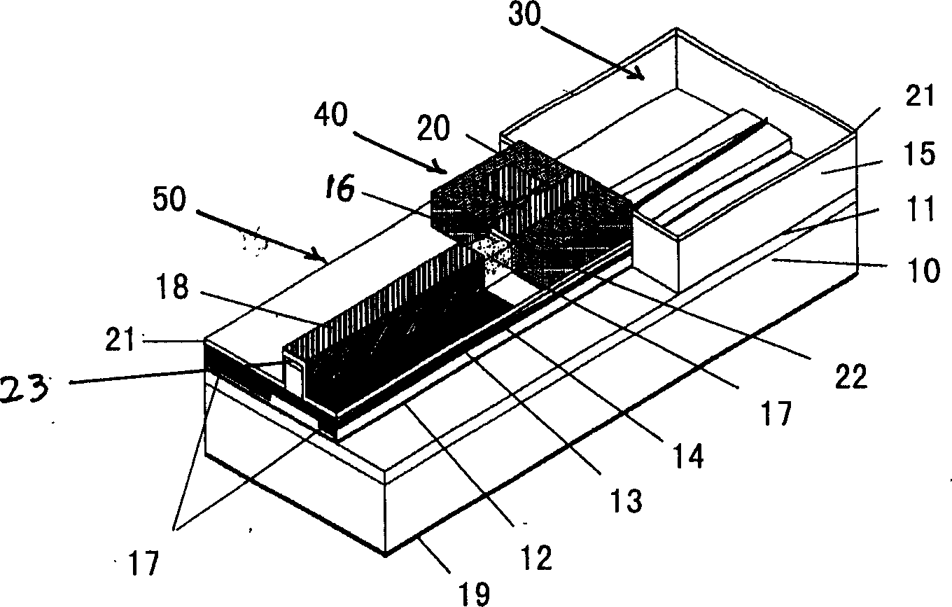
[0090] The present invention relates to a kind of preparation method of LD-EA-SSC, comprises following preparation steps:

[0091] 1. Take a 2-inch n-InP substrate and undergo strict decontamination (sequentially use ethanol, trichlorethylene, acetone, ethanol to heat and boil) → pickling (soak in concentrated sulfuric acid for 1 to 2 minutes) → water washing (rinse with deionized water More than 50 times) → after drying treatment, put it into the growth chamber, the growth temperature is 655°C, the growth pressure is 22mbar, and the graphite boat rotates at 75-80 rpm. The growth rate is 0.4-0.7nm / s.

[0092] 2. On the n-type indium phosphide substrate (100) epitaxially grow n-type indium phosphide buffer layer (0.5μm thick), lower waveguide layer (thickness 50nm, bandgap wavelength 1.1μm), 0.2μm indium phosphide Space layer, thin 1.1Q layer (30nm);

[0093] 3. Using PECVD technology to grow 150nm thick SiO on the 1.1Q layer 2 , and at the same time use the corresponding ph...


PUM

PropertyMeasurementUnit
Thicknessaaaaaaaaaa
Wavelengthaaaaaaaaaa
Thicknessaaaaaaaaaa

Abstract

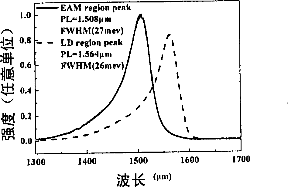
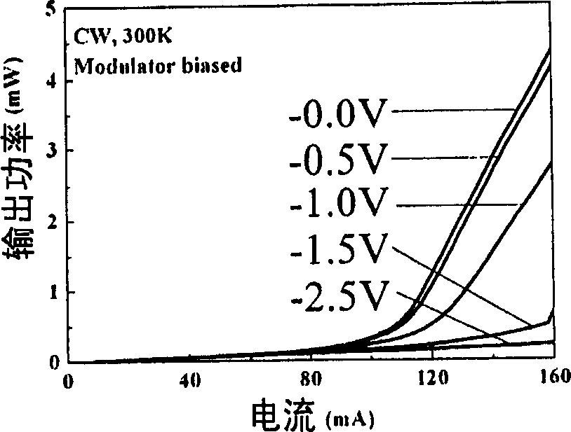
The manufacture method for laser-electroabsorption modulator-analog spot converter comprises: epitaxial growing a buffer layer, a lower waveguide layer, a space layer and an intrinsic layer by turns on substrate; growing silicon dioxide on intrinsic layer with PECVD technique; removing the intrinsic layer for second growth for source zone and intrinsic layer, etching the upper / lower waveguide structure of analog spot converter; epitaxial growing for third time thin P-type indium phosphide layer and cover layer and ohmic contact layer; re-etching the single ridge strip guidewave structure for laser and electroabsorption modulator; etching isolation channel for injecting He+; removing In-Ga-As contact layer of analog spot converter; growing silicon dioxide insulation layer by thermal oxidation method; depositing polyimide onsides of said modulator; opening the electrode window and etching the electrode figure for laser and modulator; sputtering P electrode; reducing the substrate of extension plate to cleavage into die after sputtering N electrode.

Description

technical field [0001] The invention relates to a method for manufacturing a novel semiconductor laser, an electroabsorption modulator and a spot converter single-chip integrated device through common wet etching and photolithography techniques. Background technique [0002] With the development of modern information society, the high-speed transmission, processing and storage of ultra-large capacity and long-distance information is a key technology. Whether it is the backbone network of long-distance communication, wide area network, or local area network of short-distance communication, access network, short-distance data connection optical switching, etc., a large number of high-performance and low-cost optoelectronic devices are required to support the network functions. In the application of the access network, the specific requirements for the optical transmission module are (see Optical and quantumElectronics, Vol30, 1998, pp.3284-3293): (1) low-cost modules, includin...

Claims


Application Information

Patent Timeline
IPC IPC(8): H01S5/026H01S5/00
Inventor 侯廉平王圩朱洪亮周帆王鲁峰边静
Owner INST OF SEMICONDUCTORS - CHINESE ACAD OF SCI
Learn More