Single-target magnetic control sputtering process for Cu1-xCrx alloy film
A cu1-xcrx and gu1-xcrx technology, applied in the field of single-target magnetron sputtering Cu1-xCrx alloy thin films, can solve the problems of undiscovered Cu(Cr) alloy thin films, uneven composition of alloy thin films, and high equipment requirements, reaching Improve the anti-electromigration performance, improve the purity of the film, and the effect of simple preparation process
- Summary
- Abstract
- Description
- Claims
- Application Information
AI Technical Summary
Problems solved by technology
Method used
Image
Examples
example 1
[0025] (1) Target preparation
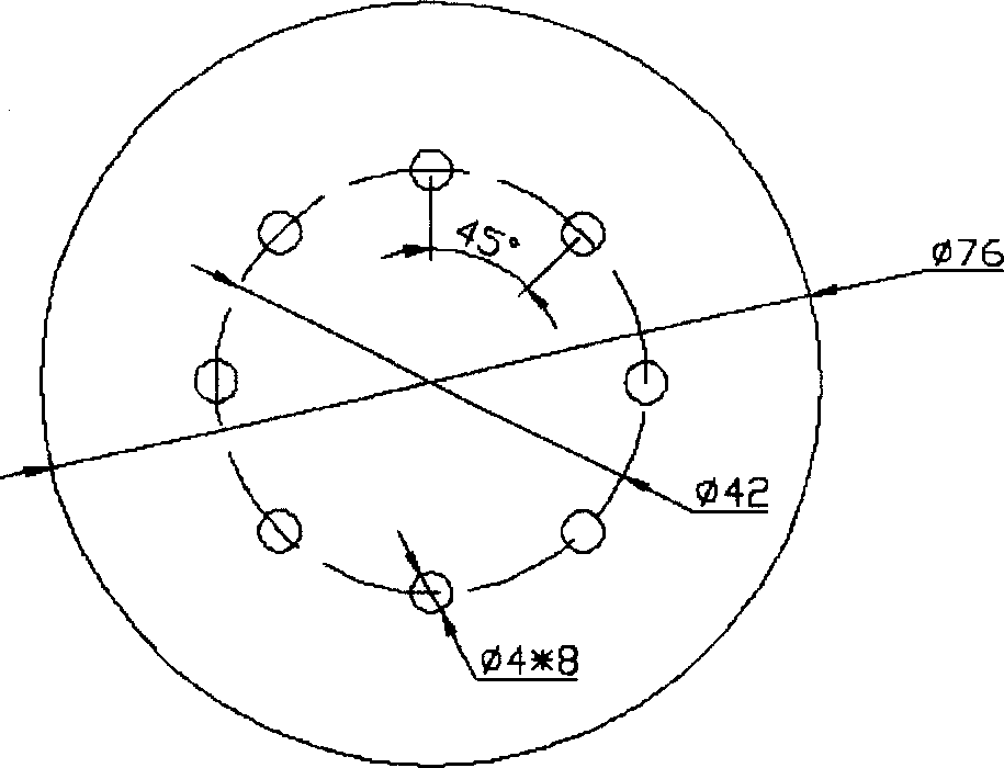
[0026] After the copper plate with a purity of 99.99% is processed and drilled as described in the specific step description (1) of the inventive method, 8 99.9% chromium metal rods of Φ4mm are polished, cleaned with acetone and alcohol Fills all small holes in the copper target and achieves a tight fit. The schematic diagram of the target is as figure 1 shown. Then the entire target and blank were cleaned with acetone, deionized water and alcohol, and dried. From the specific size of the target and the molar volume conversion of copper-chromium element, it can be known that the nominal design composition of the target in the effective sputtering area is Cu-4.04at%Cr. figure 1 It is a schematic diagram of the appearance shape of the target.
[0027] (2), substrate preparation
[0028] A (100)-oriented polished silicon single wafer was used as the substrate. The silicon substrate was cleaned with analytical pure acetone before use, then soa...
example 2
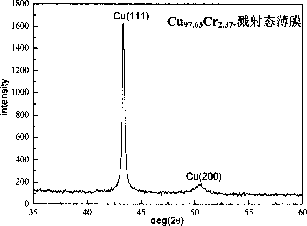
[0037] Repeat steps 1 to 4 in Example 1 (change parameters to be 4.5 × 10 -6 Torr, the sputtering time is 120min, and the sputtering power is still 100W. ). The composition of the prepared film was tested by EDX as Cu-2.37at%Cr, that is, the sputtering yield ratio of chromium and copper elements was 0.57, which was basically consistent with the 30min sputtering process. The film thickness was 855 nm. The resistivity of the original deposited film was measured by a resistance meter to be 20.434Ω·cm
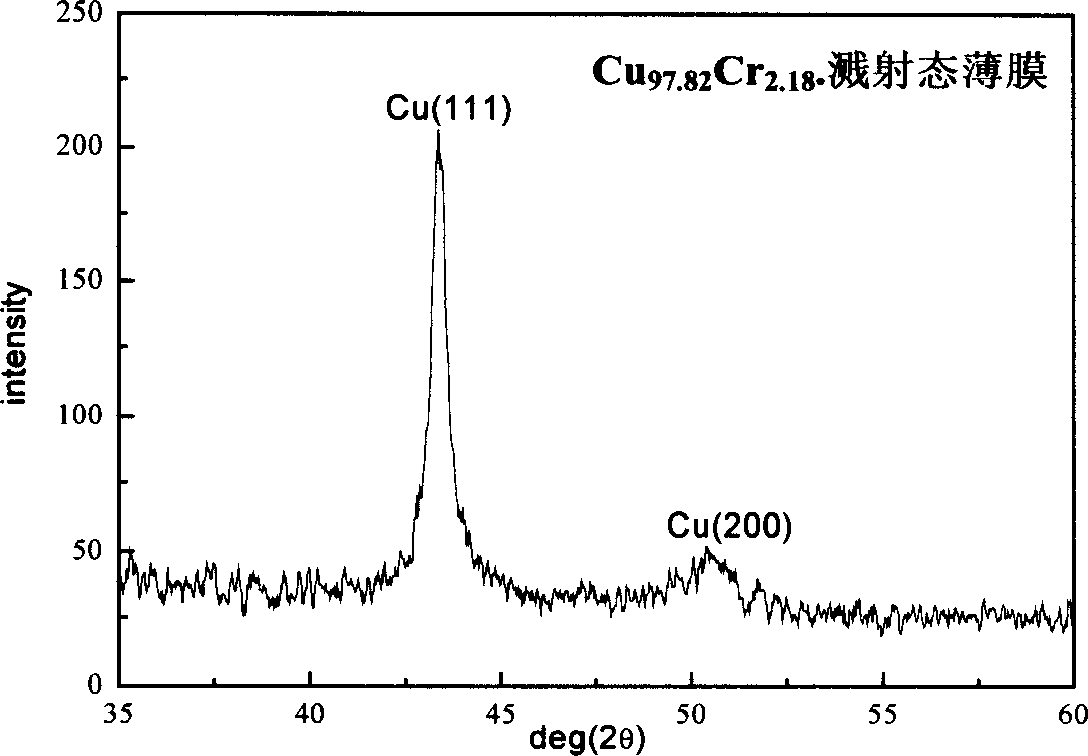
[0038] The initial structure of the film is as image 3 shown. and figure 2 In comparison, the XRD peaks are basically the same, but the intensity ratio of (111) peak to (200) peak is larger. It shows that the film has a stronger (111) texture.
[0039] (111) Texture enhancement is conducive to improving the mechanical properties of the film, improving the corrosion resistance and electromigration resistance of the film, etc.
[0040] Observation of the surface morphology ...
example 3
[0042] (1) Target preparation
[0043] Using the pure copper target processed and prepared in Example 1, after polishing four 99.9% chromium metal rods of Φ4mm, wash with acetone and alcohol to fill all the small holes in the copper target and achieve a tight fit. Four small chromium rods are evenly distributed in the hole at a 90° angle to each other. Then the entire target and blank were cleaned with acetone, deionized water and alcohol, and dried. From the specific size of the target and the molar volume of copper-chromium element, it can be known that the nominal design composition of the target in the effective sputtering area is Cu-4.04at%Cr.
[0044] (2), substrate preparation
[0045] The specific steps of substrate preparation are described in Example 1.
[0046] (3) Thin films prepared by sputtering
[0047] The baffle, target and substrate were sequentially loaded into CEVP Gamma 1000c multi-target magnetron sputtering apparatus. After 5 minutes of pre-sputteri...
PUM
| Property | Measurement | Unit |
|---|---|---|
| diameter | aaaaa | aaaaa |
| thickness | aaaaa | aaaaa |
| thickness | aaaaa | aaaaa |
Abstract
Description
Claims
Application Information


