Gas phase synthesis process of nanometer particle array with one-dimensional diameter and number density gradient
A nanoparticle and gas-phase synthesis technology, applied in the field of gas-phase synthesis of nanoparticle arrays, can solve the problems of inability to obtain nanoparticle diameter gradient distribution, high efficiency and low cost, etc., and achieve the effect of large compatibility
- Summary
- Abstract
- Description
- Claims
- Application Information
AI Technical Summary
Problems solved by technology
Method used
Image
Examples
Embodiment 1
[0033] Embodiment 1. has the gas-phase synthesis method of the nanoparticle array of the gradient distribution of single size and number density, and its synthetic steps are as follows:
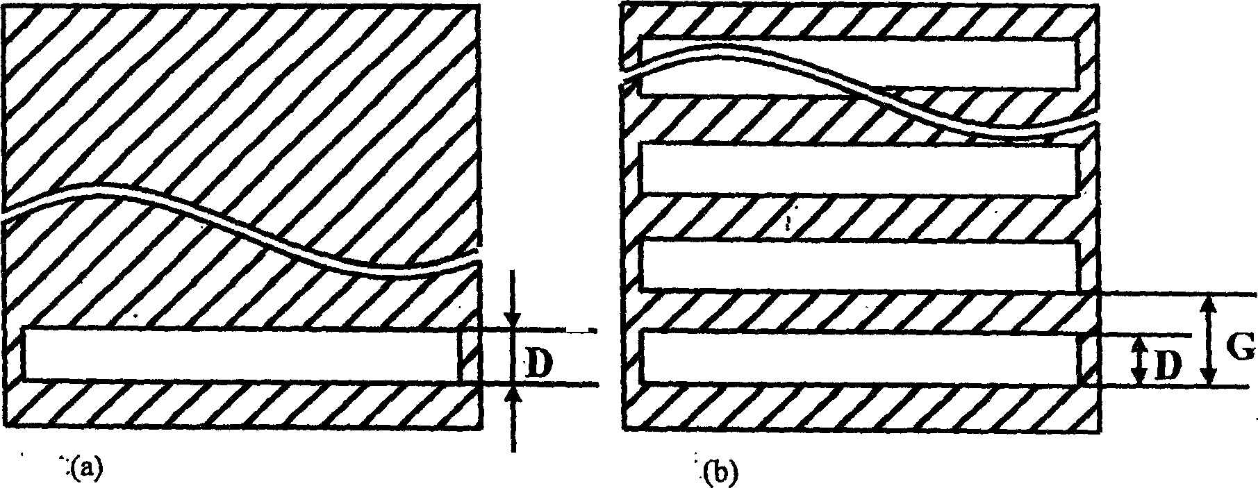
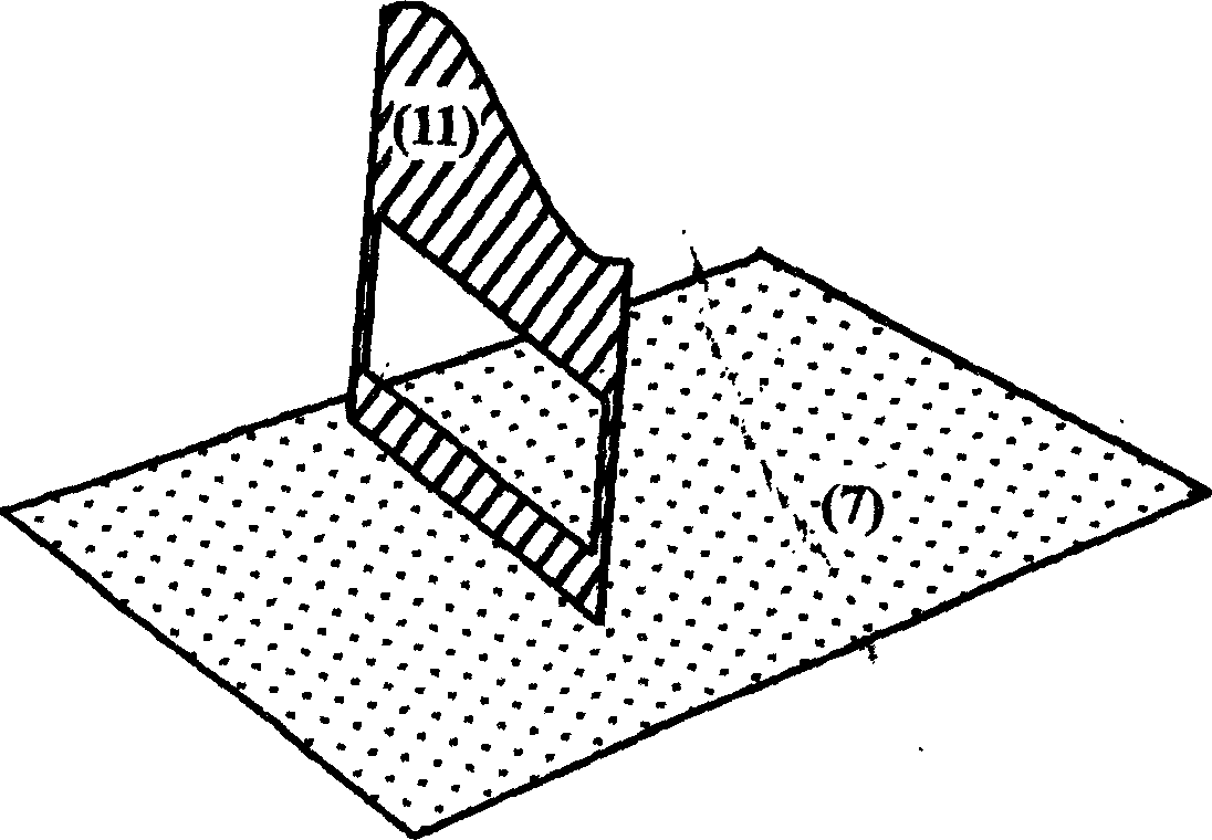
[0034] (1) Use mica flakes about 1 micron thick to press figure 2 The structure of (a) is used to make a blocking mask (11), the mask is 20mm wide, 20mm high, and the transmission window width is 3 microns, 3 microns apart from the bottom end of the mask, and the mask (11) is pressed image 3 The configuration is vertically placed close to the surface of the amorphous carbon film substrate (7), and fixed on the rotatable substrate holder, and then the substrate holder is sealed in a suitable position in the high vacuum deposition chamber (6);
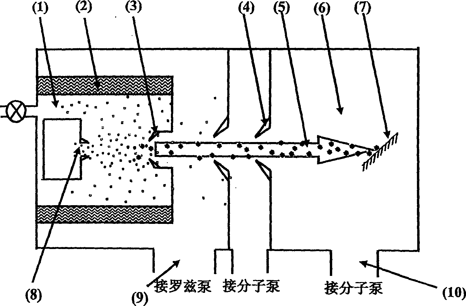
[0035] (2) adopt magnetron plasma gas phase aggregation source to produce tin nanoparticles, in the condensation chamber (2) of liquid nitrogen cooling, produce high-density tin atoms by magnetron sputtering (8) under the argon gas pressure of 200Pa, ti...
Embodiment 2
[0040] Embodiment 2. has the gas-phase synthesis method of the nanoparticle array of size and number density gradient that repeats alternately, and its synthetic steps are as follows:
[0041] (1) Use a stainless steel sheet with a thickness of about 2 microns to press figure 2 The structure of (b) makes a blocking mask (11), the mask is 20mm wide and 20mm high, the width of each transmission window is 3 microns, the bottom transmission window is 3 microns from the bottom of the mask, and the repetition period of the transmission windows is 5 Micron, the mask (11) is pressed image 3 The configuration is vertically placed close to the surface of the substrate (7) of the monocrystalline silicon wafer, and fixed on the rotatable substrate holder, and then the substrate holder is sealed in an appropriate position in the high vacuum deposition chamber (6);
[0042] Steps (2), (3), (4), (5) are the same as in Example 1;
[0043] (6) control the nanoparticle beam current (5) afte...
PUM
| Property | Measurement | Unit |
|---|---|---|
| thickness | aaaaa | aaaaa |
| diameter | aaaaa | aaaaa |
Abstract
Description
Claims
Application Information


