YAG chip-type white-light light-emitting-diode and its packing method

A light-emitting diode and chip-type technology, applied in the field of white light LED, can solve the problems of poor uniformity of white light, and achieve the effects of stable high-temperature performance, simple technical solution, and mature preparation technology

Active Publication Date: 2006-08-09
SUN YAT SEN UNIV +2
View PDF2 Cites 37 Cited by
  • Summary
  • Abstract
  • Description
  • Claims
  • Application Information

AI Technical Summary

Problems solved by technology

[0006] The purpose of the present invention is to solve the technical problem of poor white light uniformity of current whit

Method used


Image

  • YAG chip-type white-light light-emitting-diode and its packing method
  • YAG chip-type white-light light-emitting-diode and its packing method
  • YAG chip-type white-light light-emitting-diode and its packing method

Examples


Embodiment 1

[0025] (1) Growth of single crystal phosphor cerium yttrium aluminum garnet:

[0026] According to the chemical composition expression Y 2.97 al 5 o 12 : 0.03Ce (x=0, y=0, m=0.01, n=0) weighing

[0027] Y 2 o 3 : 335.34g

[0028] al 2 o 3 : 254.9g

[0029] CeO 2 : 5.16g

[0030] Grinding and mixing evenly, and then roasting under a hydrogen atmosphere; then placing the roasted product in an Ir iridium crucible of an intermediate frequency furnace, and growing a single crystal phosphor cerium yttrium aluminum garnet by pulling method under an Ar atmosphere.

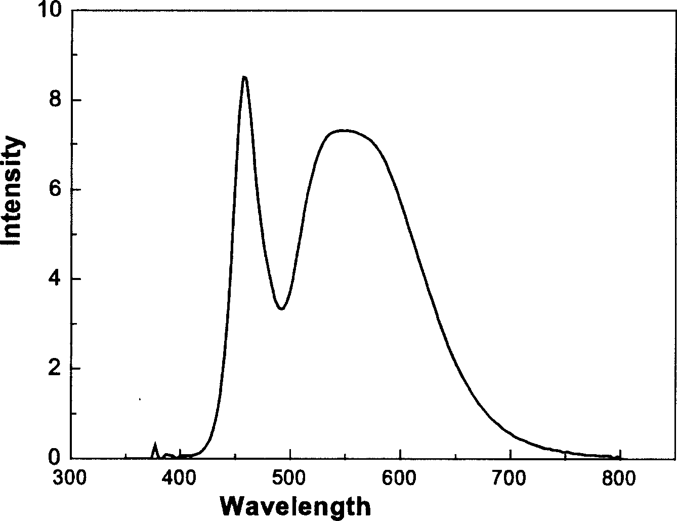
[0031] (2) Post-treatment of the single crystal phosphor cerium yttrium aluminum garnet: cutting the single crystal phosphor cerium yttrium aluminum garnet obtained above to obtain a circular single wafer with a thickness of 0.1 mm, and then the single wafer Perform single-side polishing treatment to finally obtain the desired sheet-type single crystal phosphor cerium yttrium aluminum garnet.

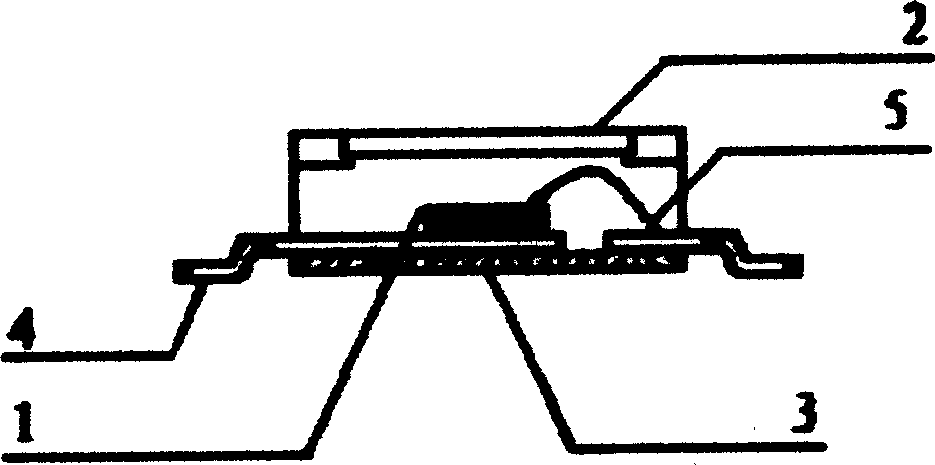
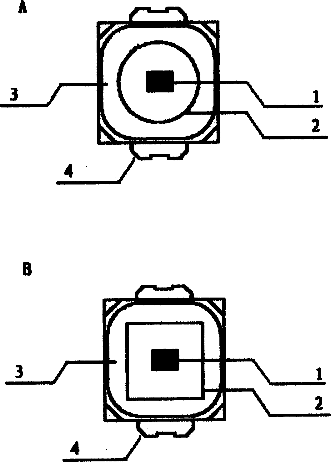
[0032] (3) Packagi...

Embodiment 2

[0034] (1) Growth of single crystal phosphor cerium yttrium aluminum garnet:

[0035] According to the chemical composition expression (Y 0.3 Gd 0.5 ) 3 (Ga 0.5 Al 0.5 ) 5 o 12 : 0.3Ce, 0.3Pr (x=0.5, y=0.5, m=0.1, n=0.1) weighed

[0036] Y 2 o 3 : 101.62g Gd 2 o 3 : 271.95g

[0037] Al 2 o 3 : 127.45g Ga 2 o 3 : 234.3g

[0038] CeO 2 : 51.63g Pr 6 o 11 : 51.07g is ground and mixed evenly, and then roasted under hydrogen atmosphere; then the roasted product is placed in the Ir iridium crucible of intermediate frequency furnace, and grown by pulling method under Ar atmosphere to obtain single crystal phosphor cerium yttrium aluminum pomegranate stone.

[0039] (2) Post-processing of the single crystal phosphor cerium yttrium aluminum garnet: cutting the single crystal phosphor cerium yttrium aluminum garnet obtained above to obtain a square single wafer with a thickness of 1.0 mm, and then performing Double-sided polishing treatment finally obtains the desir...

Embodiment 3

[0042] (1) Growth of single crystal phosphor cerium yttrium aluminum garnet:

[0043] According to the chemical composition expression (Y 0.71 Gd 0.2 ) 3 (Ga 0.3 Al 0.7 ) 5 o 12 : 0.15Ce, 0.12Sm (x=0.2, y=0.3, m=0.05, n=0.04) weighing

[0044] Y 2 o 3 : 240.5g Gd 2 o 3 : 108.78g

[0045] Al 2 o 3 : 178.43g Ga 2 o 3 : 140.58g

[0046] CeO 2 : 25.82g Sm 2 o 3 : 20.93g is ground and mixed evenly, and then roasted under hydrogen atmosphere; then the roasted product is placed in the Ir iridium crucible of intermediate frequency furnace, and grown by pulling method under Ar atmosphere to obtain single crystal phosphor cerium yttrium aluminum pomegranate stone;

[0047] (2) Post-treatment of the single crystal phosphor cerium yttrium aluminum garnet: cutting the single crystal phosphor cerium yttrium aluminum garnet obtained above to obtain a single wafer with a thickness of 0.55mm, and then double-cutting the single wafer. The surface is not polished, and finall...


PUM

PropertyMeasurementUnit
Thicknessaaaaaaaaaa
Thicknessaaaaaaaaaa
Thicknessaaaaaaaaaa

Abstract

Using YAG single crystal body converts part of blue light sent from GaN based semiconductor LED crystal grain to another light in one or more ideal wave bands. Then, not converted remanent blue light sent from LED crystal grain is mixed with the converted light in ideal wave band to generate white light. Through controlling each parameter of fluorophor of single crystal chip, the method adjusts and controls proportion between yellow light converted by the fluorophor of single crystal and not converted blue light. At the same time, using evenness of single crystal chip obtains even white light in high quality. Comparing with traditional technique, the invention solves difficult issue of controlling dispersivity of powder of fluorophor in sealant in silicone greases or resins. After wafer is cut to chips in desired size, packaging operation is full automatic so as to raise degree of mechanization.

Description

technical field [0001] The invention relates to the field of white light LEDs, in particular to a YAG chip type white light light emitting diode and a packaging method thereof. Background technique [0002] With breakthroughs in the key technical fields of high-efficiency violet and blue light-emitting diodes, white light LEDs have increasingly become the focus of attention. At present, the technical solutions for obtaining white light LEDs are mainly divided into LED chip combination and fluorescent conversion, and the latter is currently the mainstream technology in the field of white light LEDs. Among them, the industrialized white LED is mainly composed of blue LED chip and phosphor Y 3 al 5 o 12 : Ce 3+ (YAG:Ce), the main preparation technology is to mix the phosphor and colloid in a certain proportion to form a slurry, and then directly or indirectly coat the slurry on the surface of the blue LED grain by coating or dispensing, and finally Curing and molding at a ...

Claims


Application Information

Patent Timeline
IPC IPC(8): H01L33/00H01L33/50
CPCH01L2224/48091H01L2224/48247
Inventor 苏锵谢鸿波方福波王静钟玖平李绪锋吴昊武南平潘利兵李军政
Owner SUN YAT SEN UNIV
Why Eureka
Try Eureka