Complex alloy thin film with hydrogen-inducing off-coloring function and production thereof
A multi-element alloy and alloy thin film technology, applied in the field of functional materials, can solve problems such as poor hydrogen absorption and desorption kinetics, poor optical properties, and poor film stability
- Summary
- Abstract
- Description
- Claims
- Application Information
AI Technical Summary
Problems solved by technology
Method used
Image
Examples
Embodiment 1
[0035] 1) Preparation of bulk alloy
[0036] At room temperature and under a protective atmosphere of nitrogen or argon, weigh 1:1, 1:3 and 3:1 molar amounts of La and Ni, and then use induction heating under high vacuum for melting to make LaNi, La 3 Ni and LaNi 3 bulk alloy. In order to ensure the uniformity of the composition, the solidified alloy is turned over, smelted repeatedly, and finally the obtained bulk alloy is prepared such as figure 1 shown.
[0037] 2) Thin film deposition
[0038] The smelted LaNi alloy and pure Mg were put under ultra-high vacuum conditions (10 -9 Pa), by electron beam evaporation, the multilayer film with ABABAB structure is deposited by evaporation. Among them, each layer of LaNi is 1.5nm, a total of 25 layers; each layer of Mg is 1.5nm, a total of 25 layers.
[0039] 3) Thin film protective layer
[0040] A nickel protective layer was deposited on the surface of the film by sputtering, with a thickness of 2 nm. The prepared films a...
Embodiment 2
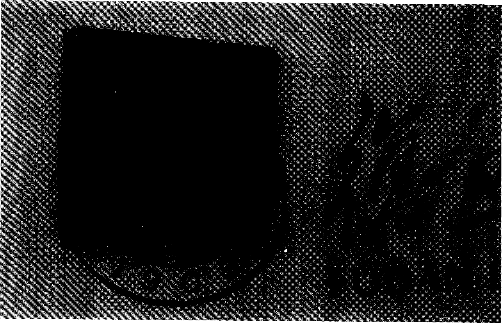
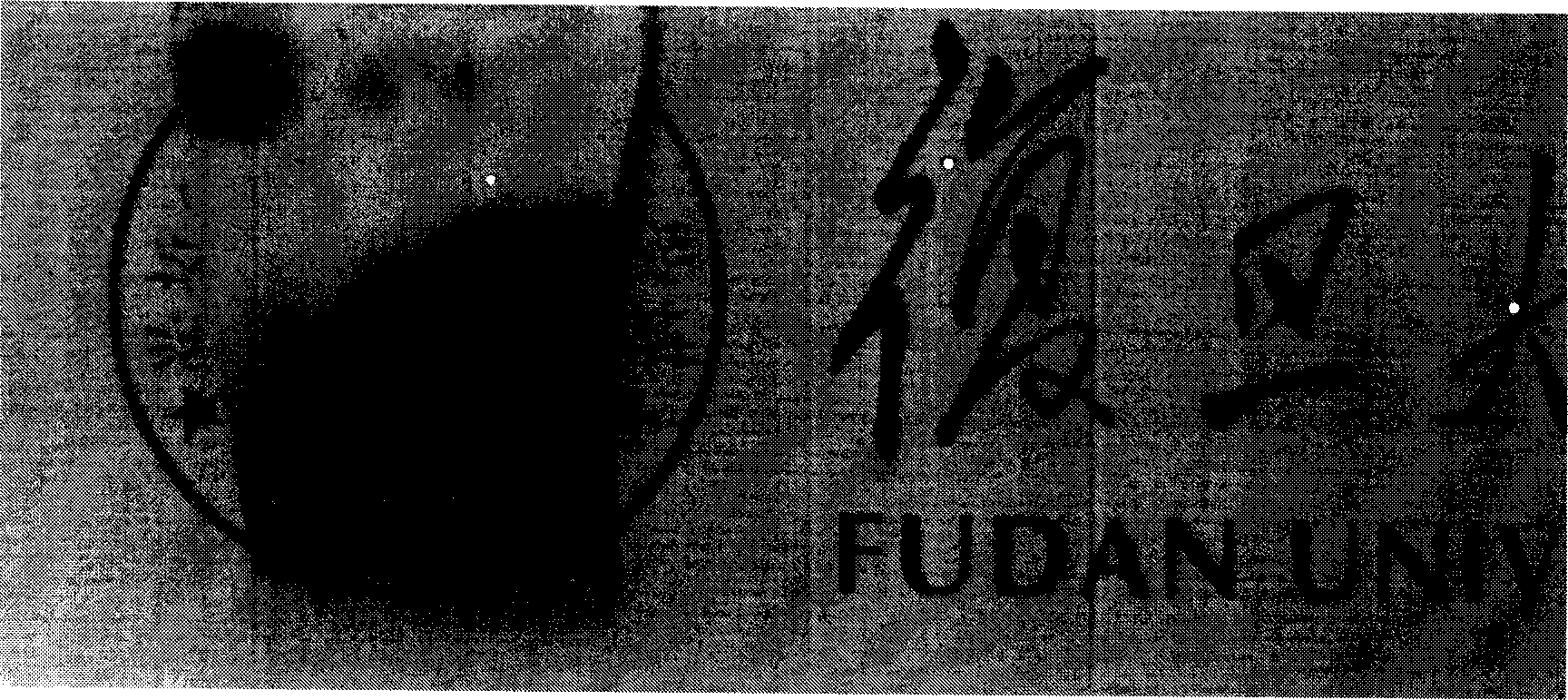
[0044] Taking the prepared LaMgNi alloy thin film as an example, the alloy thin film is hydrogenated as Figure 4 shown. Figure 4 In the middle, the badge of Fudan University under the film is clearly visible. The film is colorless and transparent, with high transmittance and low reflectance and absorptivity. Figure 5 The change of transmittance before and after hydrogenation was compared. It can be seen from the figure that the transmittance of the film before hydrogenation is almost zero, and the maximum transmittance reaches 50% after hydrogenation, and the average transmittance is 45% in the wavelength range from 400nm to 900nm. The alloy thin film of the invention has high transmittance in the range of visible light and can meet the requirements of practical application.
PUM
 Abstract
Description
Claims
Application Information


