Detector converted on infrared wavelength, near-infrared wavelength

A near-infrared and detector technology, applied in the field of infrared-near-infrared wavelength up-conversion detectors, can solve the problems of short carrier lifetime, small absorption coefficient, low quantum efficiency, etc., and achieves improved area array scale and high responsivity , Good material uniformity

Active Publication Date: 2006-12-06
SHANGHAI INST OF TECHNICAL PHYSICS - CHINESE ACAD OF SCI
View PDF0 Cites 10 Cited by
  • Summary
  • Abstract
  • Description
  • Claims
  • Application Information

AI Technical Summary

Problems solved by technology

[0004] However, the main shortcomings of the current quantum well infrared detectors are: low quantum efficiency due to small material absorption coefficient for normal incident radiation, low responsivity due to short carrier lifetime and large dark current, etc.

Method used


Image

  • Detector converted on infrared wavelength, near-infrared wavelength
  • Detector converted on infrared wavelength, near-infrared wavelength

Examples


Embodiment Construction

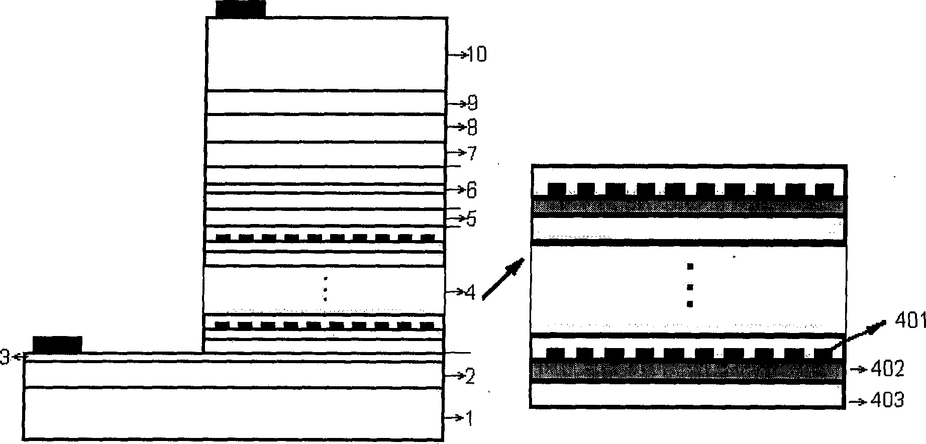
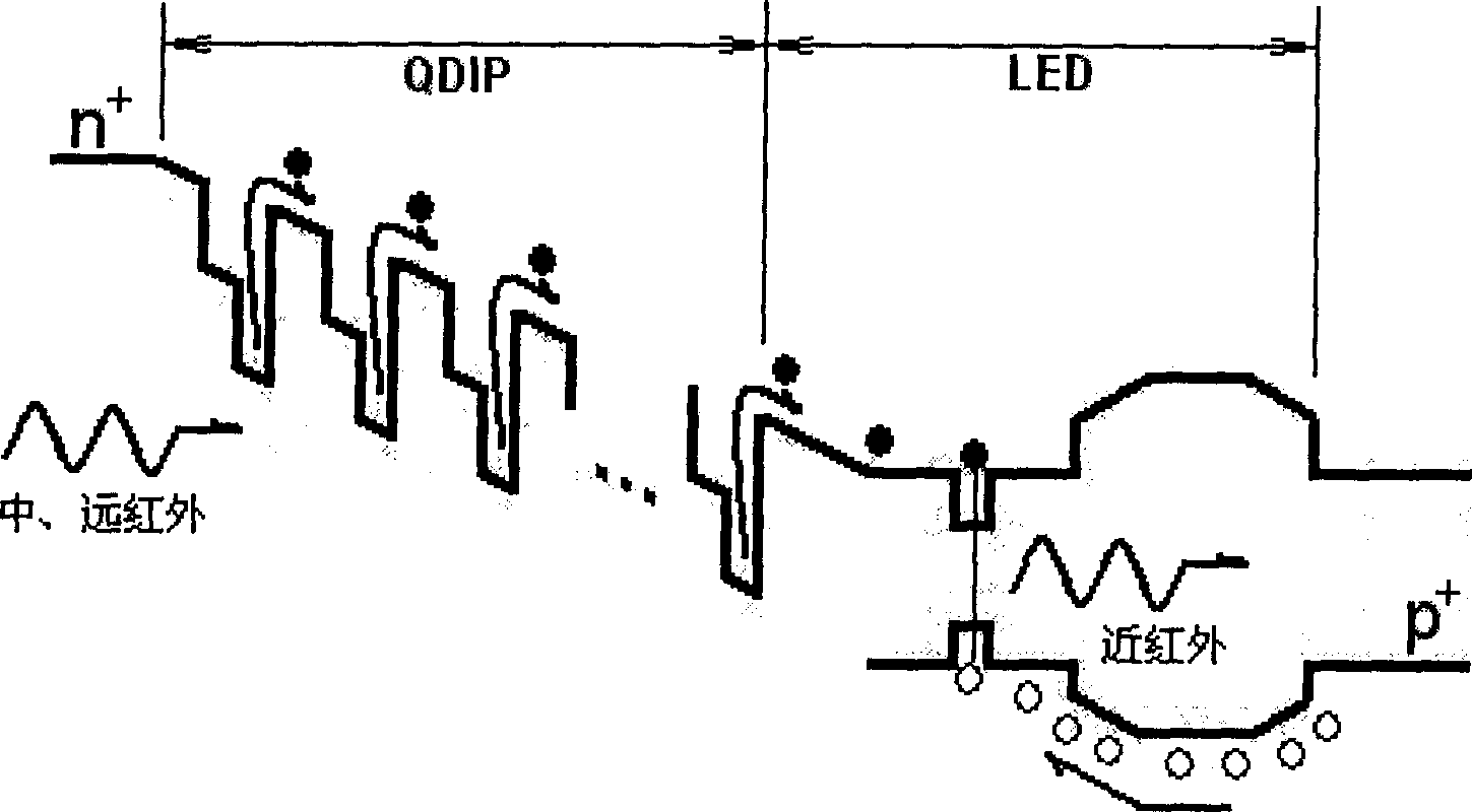
[0023] Below with the infrared absorption peak of QDIP being set near 8~9 microns, the peak wavelength of the EL spectrum of LED is embodiment at 870nm, in conjunction with accompanying drawing concrete structure of the present invention is described in further detail:

[0024] The detector of the present invention utilizes a typical technique of semiconductor material epitaxy, such as molecular beam epitaxy, to grow in sequence on a semi-insulating GaAs substrate 1:

[0025] no * -GaAs lower electrode layer 2 with a thickness of 800 nm and a doping concentration of 1.5×10 18 cm -3 ;

[0026] The intrinsic GaAs spacer layer 3 has a thickness of 5 nm;

[0027] 2 atomic layers of InAs quantum dot layer 401 and 20 atomic layers of In are alternately grown for 10 cycles y Ga 1-y As potential well layer 402 and GaAs barrier layer 403 of 130nm thick atomic layer, thus forming a quantum dot infrared detector 4, the average density of InAs quantum dots is 100-120 / μm 2 , the y va...


PUM

PropertyMeasurementUnit
thicknessaaaaaaaaaa

Abstract

The invention discloses infrared-near-infrared wavelength conversion detector which can integrate InAs multi-quantum point infrared detector and light-emitting diode into one chip. The former is made up of InAs/InyGa1-yAs/GaAs which alternately grows for ten cycles. The latter is made up of GaAs barrier layer and InzGa1-zAs active potential well layer. It can transform long wave thermal infrared to near infrared light without grating. This can simplify detecting system structure. The used material has mature preparation technology and good uniformity.

Description

technical field [0001] The invention relates to a quantum dot infrared detector and a light-emitting diode, in particular to an infrared-near-infrared wavelength up-conversion detector that effectively integrates a quantum dot infrared detector (QDIP) and a light-emitting diode (LED) on the same chip. Background technique [0002] Traditional infrared detectors mostly use focal plane array technology. The signal of each photodetection unit in the array is sent to an external silicon readout circuit and converted into a video signal for output. This structure requires each photosensitive element to form a corresponding interconnect point on the silicon readout circuit. Therefore, it is necessary to accurately convert the information on the focal plane array to a correspondingly large number of interconnected nodes. Integrated systems between dissimilar materials are expensive and unreliable, and are especially susceptible to thermal shock from refrigeration and non-refriger...

Claims


Application Information

Patent Timeline
Patent Type & Authority Applications(China)
IPC IPC(8): G01N21/25G01J1/00
Inventor 陆卫刘昭麟甄红楼李宁李志锋陈平平张波陈效双
Owner SHANGHAI INST OF TECHNICAL PHYSICS - CHINESE ACAD OF SCI
Why Eureka
Try Eureka