

Heterojunction pn diode based on silicon nanoline and producing method thereof
A silicon nanowire and pn junction technology, applied in the fields of nanomaterials and electronic materials, can solve problems that have not been reported before, and achieve the effects of increasing the recombination probability, low forward turn-on voltage, and large specific surface area.
- Summary
- Abstract
- Description
- Claims
- Application Information
AI Technical Summary
Problems solved by technology
Method used
Image

Examples
Embodiment 1
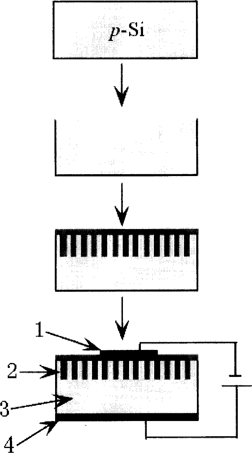
[0016] The preparation process will be described in detail below by taking a single-side polished (100) oriented silicon wafer as an example.
[0017] (1) Cleaning: The silicon wafer used in this example is a single-side polished (100) oriented silicon wafer. The method of No. 1 solution and No. 2 solution commonly used in semiconductor technology is used to clean the silicon wafer. The formula of No. 1 liquid is: concentrated ammonia water: 30% hydrogen peroxide: deionized water = 1: 2: 7; the formula of No. 2 liquid is: concentrated hydrochloric acid: 30% hydrogen peroxide: deionized water = 1: 2: 7. First boil the silicon chip with No. 1 liquid, make it boil for a while, wait for it to cool down, and then clean it with deionized water. Then put in the No. 2 solution to boil the silicon chip, make it boil for a while, wait for it to cool down, take it out, clean it with deionized water, and finally dry it.
[0018] (2) Preparation of p-type silicon nanowires: A polytetraf...
Embodiment 2
[0022] The preparation process will be described in detail below by taking a single-side polished (100) oriented silicon wafer as an example.
[0023] (1) Cleaning: The silicon wafer used in this example is a single-side polished (100) oriented silicon wafer. The method of No. 1 solution and No. 2 solution commonly used in semiconductor technology is used to clean the silicon wafer. The formula of No. 1 liquid is: concentrated ammonia water: 30% hydrogen peroxide: deionized water = 1: 2: 7; the formula of No. 2 liquid is: concentrated hydrochloric acid: 30% hydrogen peroxide: deionized water = 1: 2: 7. First boil the silicon chip with No. 1 liquid, make it boil for a while, wait for it to cool down, and then clean it with deionized water. Then put in the No. 2 solution to boil the silicon chip, make it boil for a while, wait for it to cool down, take it out, clean it with deionized water, and finally dry it.
[0024] (2) Preparation of p-type silicon nanowires: A polytetraf...
PUM
| Property | Measurement | Unit |
|---|---|---|
| Diameter | aaaaa | aaaaa |
Abstract
Description
Claims
Application Information