Method for preparing L10 ordered alloy film

A technology of ordered alloys and alloy films, applied in metal material coating process, ion implantation plating, coating and other directions, to avoid grain growth, simplify the preparation process, and achieve the effect of small grain size

Inactive Publication Date: 2007-05-09
SHANGHAI INST OF TECH
View PDF0 Cites 13 Cited by
  • Summary
  • Abstract
  • Description
  • Claims
  • Application Information

AI Technical Summary

Problems solved by technology

[0003] The technical problem to be solved by the present invention is to apply the laser annealing process to L1 0 In the preparation of ordered alloy thin films, the degree of ordering of alloy thin films is controlled to avoid the traditional L1 0 High-temperature heating in the preparation of ordered alloy thin films saves energy consumption and time in the preparation process

Method used


Image

  • Method for preparing L10 ordered alloy film
  • Method for preparing L10 ordered alloy film
  • Method for preparing L10 ordered alloy film

Examples


Embodiment 1

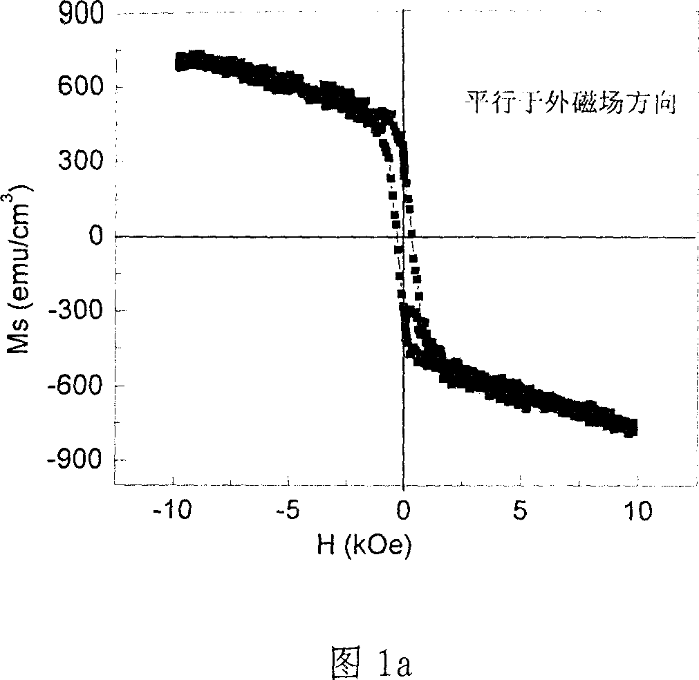
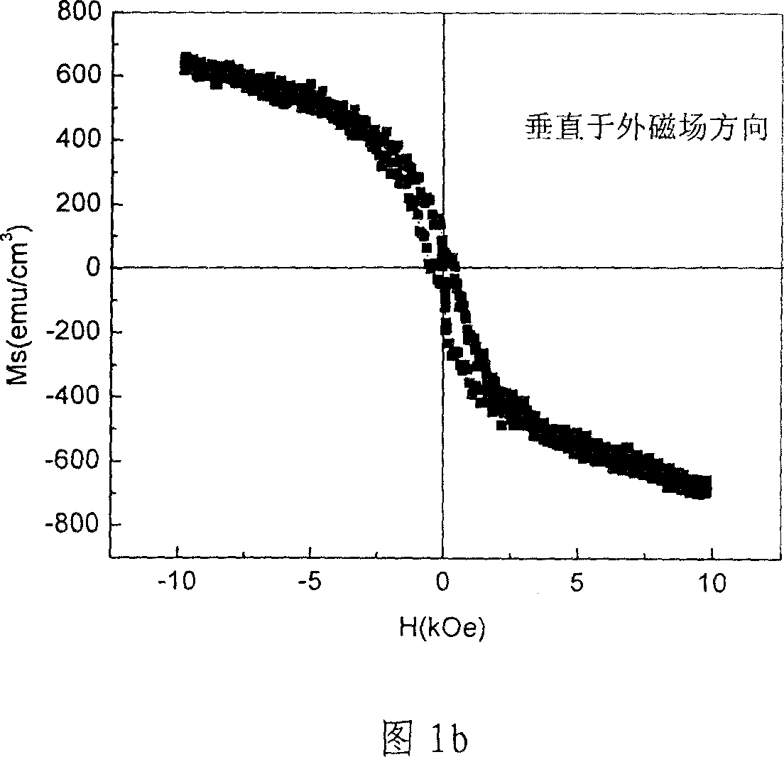
[0018] With oriented single crystal silicon wafer as the substrate, the Si / FePt / SiN three-layer film structure was prepared by magnetron sputtering. The background vacuum during sputtering is 1*10 -4 Pa, Ar is used as the sputtering gas, and the sputtering pressure is 1 Pa. The FePt film was sputtered with a DC composite target, the sputtering power was 25W, the sputtering time was 10min, the diameter of the Fe target was Φ50, the size of the Pt piece was 5*5mm, and the purity was 99.99%. The SiN film as a protective layer is sputtered by radio frequency reactive sputtering with Ar and N 2 Commonly used as sputtering gas, P Ar : P N2 =1:1, sputtering time is 8min. All films are prepared at room temperature. Laser annealing uses Ar with a wavelength of 514nm + The laser is used as the light source, and the laser is continuous light. The Gaussian radius of the spot is about 0.9mm. The laser scanning speed is 5mm / s, and the laser power is set to 12W. The laser light is incident from...

Embodiment 2

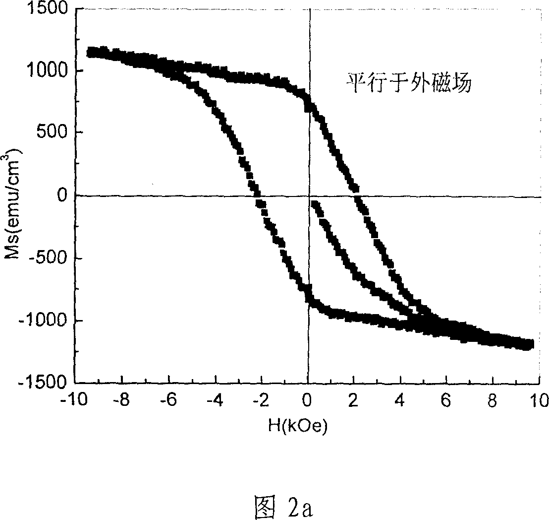
[0020] With MgO single crystal as the substrate and Pt as the buffer layer, the MgO substrate / Pt / FePt / SiN was prepared by magnetron sputtering. The preparation methods of FePt and SiN films were the same as in Example 1, and the purity of Pt film was 99.99 % Pt target DC sputtering for 5min. The laser annealing method is the same as in Example 1. Figures 3a and 3b are comparisons of X-ray diffraction patterns of the film before and after laser irradiation. It can be seen that before annealing, the FePt film has a strong (111) diffraction peak, a (001) diffraction peak is very weak, and a (002) diffraction peak does not appear, which indicates that the film has a typical fcc disordered structure at this time. After laser annealing, the intensity of the (111) diffraction peak is weakened, and the intensity of the (001) diffraction peak and (002) diffraction peak are obviously enhanced. This shows that the fct ordered phase has appeared. Further increase the laser power or slow down ...


PUM

PropertyMeasurementUnit
laser intensityaaaaaaaaaa
thicknessaaaaaaaaaa

Abstract

This invention discloses a method for preparing ordered L10 alloy thin film. The order-disorder transition of the thin film is realized by laser annealing. The laser is CO2 laser, Ar+ laser, Nd: YAG laser or excimer laser. The power intensity of the laser applied on the surface of the alloy thin film is 10-100 W/mm2. The alloy thin film is placed on a platform that can be adjusted in three dimensions and can move freely, and the scanning rate of rapid scanning is 1-10 mm/s. By this method, the alloy thin film can maintain small grain sizes and decrease interaction forces among grains while forming fct ordered structure. Compared with traditional thermal annealing method, the method has simple process, and is suitable for industrial production of ordered L10 alloy thin film.

Description

Technical field [0001] The present invention relates to an information storage disk, and more specifically to a magnetic storage medium L1 used on an information storage disk 0 Preparation method of ordered alloy film. Background technique [0002] In recent years, the density of magnetic storage has increased rapidly at a rate of 60% per year. With the continuous improvement of storage density, the size of the recording domain continues to decrease. In the near future, it will reach the theoretical limit (V∝kT) determined by superparamagnetism. / Ku). Where k is Boltzmann's constant, T is temperature, and V is the smallest magnetic domain size that can exist stably. When kT is constant, the larger the intrinsic anisotropy constant Ku, the smaller the magnetic pumping size V, and the theoretical limit density will increase accordingly. Therefore, finding a medium with a large Ku is an inevitable requirement for the development of high-density magnetic storage. L1 0 Ordered FePt al...

Claims


Application Information

Patent Timeline
Patent Type & Authority Applications(China)
IPC IPC(8): C23C14/58C21D1/26G11B3/70
Inventor 王现英干福熹
Owner SHANGHAI INST OF TECH
Why Eureka
Try Eureka