

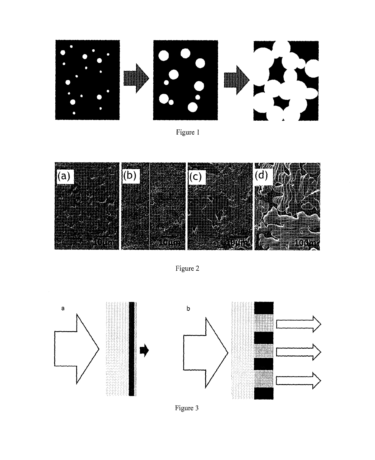
Photoactive layer production process
a photoactive layer and production process technology, applied in the direction of sustainable manufacturing/processing, final product manufacturing, sustainable buildings, etc., can solve the problems of film deterioration, unsatisfactory performance or a lower visible transmittance than desired, and limited efficiencies of fundamental charge transfer losses, etc., to achieve low cost, low cost, and high power conversion efficiency
- Summary
- Abstract
- Description
- Claims
- Application Information
AI Technical Summary
Benefits of technology
Problems solved by technology
Method used
Image

Examples
example 1
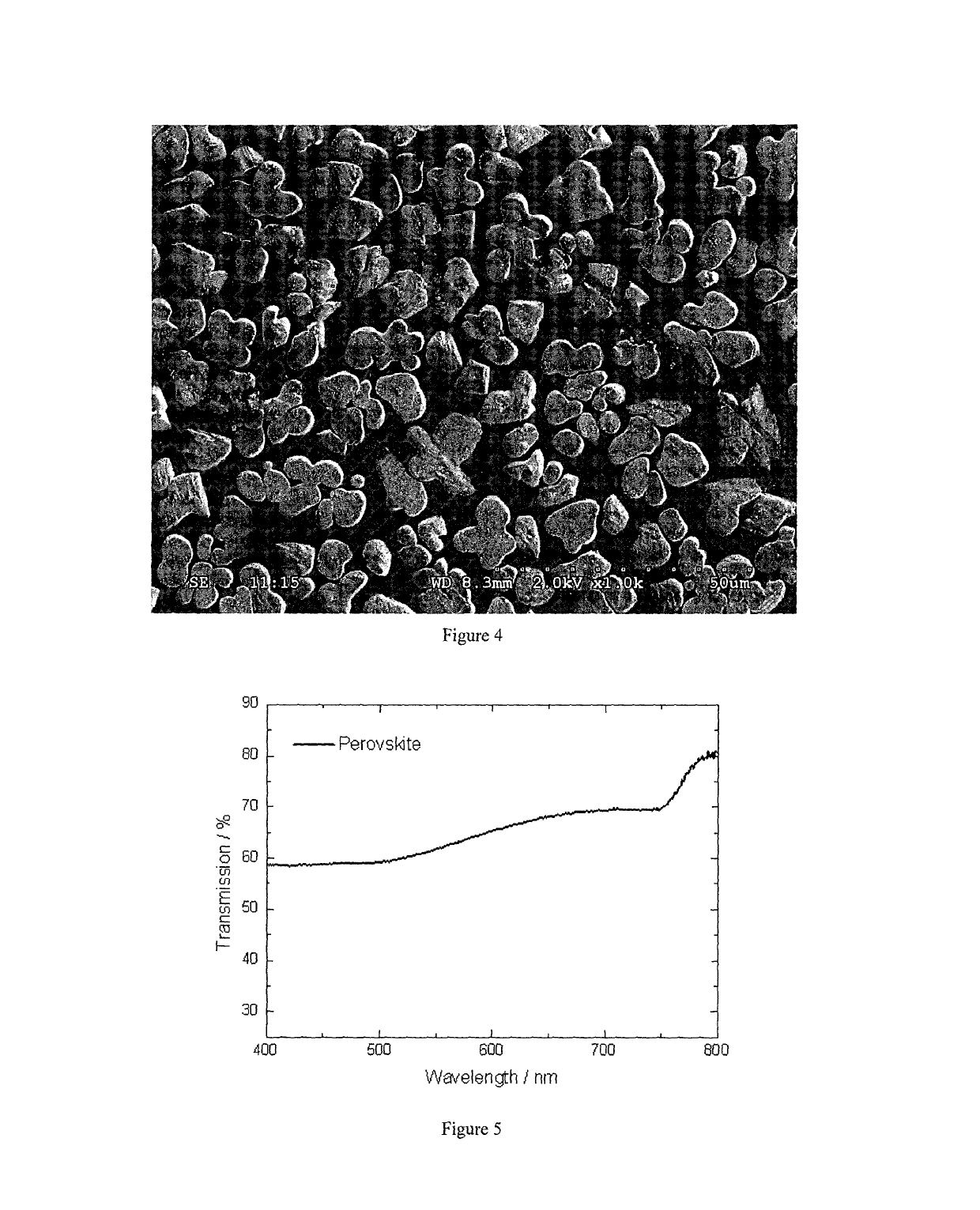
Formation of Dewet Perovskite Film
[0422]A dewet layer of perovskite, CH3NH3PbI3-xClx, was formed on a glass substrate. CH3NH3I and PbCl2 were mixed together in Dimethyl sulfoxide (DMSO) at a molar ratio of 3:1 CH3NH3I:PbCl2, to form a precursor solution. 100 μl of the precursor solution was deposited onto a clean glass slide and spin-coated at 2000 rpm for 60 seconds. The as-spun film is clear and uniform in appearance. The coated glass slide is then placed into an oven set at 150° C. for 10 minutes. During the period of time in the oven, excess solvent and organic component are lost, and crystallisation of the perovskite absorber, CH3NH3PbI3-xClx, occurs. In addition to crystallisation, dewetting of the perovskite film occurs while solvent and excess organic components are lost. The dewet layer has a ˜50% transmission with 56% perovskite coverage. FIG. 4 shows an SEM image of the dewet layer showing the self-assembled perovskite islands that can generate power.
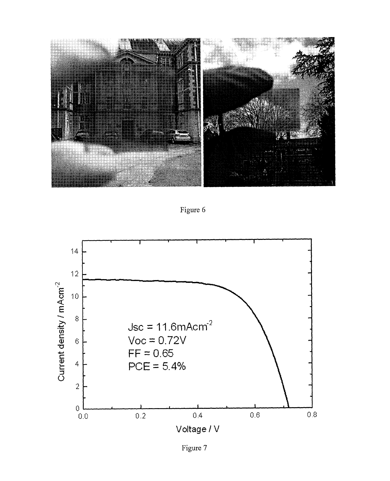
[0423]FIG. 6 shows ph...
example 2
Methods
[0446]Materials. Unless otherwise stated, all materials were purchased from Sigma-Aldrich or Alfa Aesar and used as received. Spiro-OMeTAD was purchased from Borun Chemicals. CH3NH3I was synthesised according to a reported procedure.
[0447]Semi-Transparent Perovskite Solar Cell Preparation. Devices were fabricated on fluorine-doped tin oxide (FTO) coated glass (Pilkington, 7Ω□−1). Initially FTO was removed from regions under the anode contact by etching the FTO with 2M HCl and zinc powder. Substrates were then cleaned sequentially in hallmanex detergent, acetone, propan-2-ol and oxygen plasma. A ˜50 nm hole-blocking layer of compact TiO2 was deposited by spin-coating a mildly acidic solution of titanium isopropoxide in ethanol (350 ul in 5 ml ethanol with 0.013M HCl) at 2000 rpm, and annealed at 500° C. for 30 minutes. The dewet perovskite layers were deposited by spin-coating a non-stoichiometric precursor solution of methylammonium iodide and lead chlorine (3:1 molar ratio, ...
PUM
| Property | Measurement | Unit |
|---|---|---|
| distance | aaaaa | aaaaa |
| distance | aaaaa | aaaaa |
| diameter | aaaaa | aaaaa |
Abstract
Description
Claims
Application Information