
Carbon nanotube-based thermal interface materials and methods of making and using thereof

a technology of thermal interface materials and carbon nanotubes, which is applied in the direction of electrical apparatus construction details, semiconductor/solid-state device testing/measurement, instruments, etc., can solve the problems of high contact area at such interfaces between surfaces, early termination of tube growth, and difficulty in growing very long cnts on metal substrates. achieve high levels of complian

Active Publication Date: 2019-10-29
CARBICE CORP
View PDF41 Cites 2 Cited by
  • Summary
  • Abstract
  • Description
  • Claims
  • Application Information

AI Technical Summary

Benefits of technology

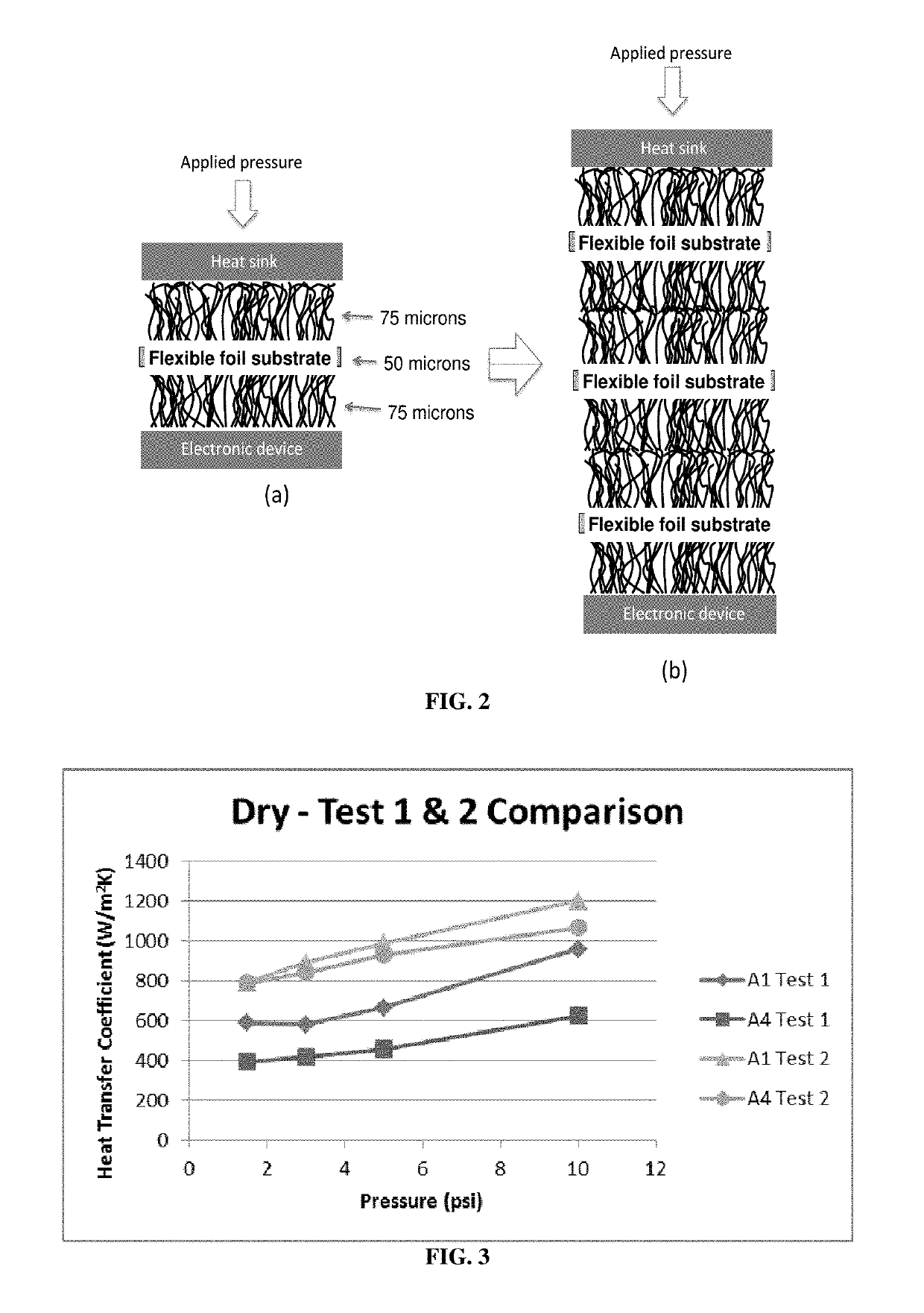
[0013]In some embodiments described, two or more CNT arrays are stacked to form multilayered or multitiered structures. Multiple CNT arrays can be stacked, such that the nanostructure elements from opposing arrays form into tiers in the stack and become at least partially interdigitated with one another. Unlike the stacking of a traditional material, stacked arrays of vertically aligned nanostructures do not suffer from a linear (or worse) increase in thermal resistance with increasing thickness. Accordingly, the resulting multilayered structures can mitigate the adverse impact of thickness and boundaries on energy transport as a result of the interdigitation of the nanostructure elements (i.e., CNTs) of the two or more arrays when contacted. In contrast, for a typical material the resistance to heat transfer is directly proportional to the material's thickness, with an additional interfacial resistance at the interfaces of a multilayered structure.
[0014]For multilayered or multitiered structures formed by stacking of vertically aligned nanostructure materials of CNT arrays, wherein the CNTs of the arrays at least partially interdigitate within or into one another, effectively increasing the density of the CNTs. Typically, the density of CNTs grown on metal substrates is only about 1% of the total volume. When two adjacent layers of CNT arrays are stacked, for example, the density of heat conducting elements, such as CNTs or structures formed thereof, is effectively doubled. As such the resistance to heat transfer per unit length is reduced in kind.
[0015]An advantage of the multilayered or multitiered structures formed by stacking of two or more CNT arrays over traditional bulk materials comes at the interface of the arrays. For example, resistance to heat transfer increases not only due to the increase in thickness of a multilayer stack, but also due to the interfacial resistances between the tiers. Accordingly, between any two adjacent tiers, the boundary between the two tiers is the location of poor heat transfer, relative to the bulk material due to poor contact between the tiers, as well as due to scattering of energy carriers (e.g. electrons or phonons) at the boundary. When interdigitated, the high aspect ratio of the nanostructures, such as CNTs, results in a very high contact area between the tiers minimizing the poor contact area contribution to the inter tier interfacial resistance. Although Kapitza (scattering) resistance cannot be completely eliminated the resistance can be reduced by applying, infiltrating, or backfilling the array or sheet with a polymer, wax, or other secondary material that facilitates thermal / energy transport across the boundary. This transport facilitation may be through the formation of a covalent or weak atomic interaction between the CNT and a secondary material, reduction of acoustic phononic transport mismatch relative to air, or other types of mechanisms.
[0022]In some embodiments the polymer, wax, liquid metal, or other suitable material can reduce the transport resistance between the multiple layers or tiers formed, resulting from improved contact area, a reduction in scattering, or other related mechanisms. In yet other embodiment the tiers formed by stacking of arrays may be bonded by use of an adhesive or a phase-change material.
[0023]CNT arrays and the multilayered or multitiered structures formed by stacking of such CNT arrays exhibit both high thermal conductance and mechanical durability. The multilayered or multitiered structures formed by stacking of CNT arrays described herein can be used as thermal interface materials (TIMs). Accordingly, such materials are well suited for applications where repeated cycling is required. For example, they can be employed as thermal interface materials during ‘burn-in’ testing of electrical components, such as chips. In some embodiments, the inert support / substrate is a surface of a conventional metal heat sink or spreader. This functionalized heat sink or spreader may then be abutted or adhered to a heat source, such as an integrated circuit package. Such TIM materials can also be placed or affixed in between a heat source and a heat sink or heat spreader, such as between an integrated circuit package and a finned heat exchanger, to improve the transfer of heat from the heat source to the heat sink or spreader.

Problems solved by technology

Furthermore, the favorable deformation mechanics of CNTs allow them to efficiently conform to the asperities of adjoining surfaces, resulting in high contact areas at such interfaces between surfaces.
A key challenge, however, in CNT-based TIMs comes from the difficulty in growing very long CNTs on metal substrates.
Unlike CNTs grown on silicon or other inert substrates, the catalyst required for CNT growth suffers from subsurface diffusion when grown on metal substrates, resulting in early termination of tube growth.
Furthermore, defects tend to accumulate in CNTs as their height increases, resulting in CNT arrays with conductivities significantly lower than the 3,000 W / m-K limit otherwise achievable with pristine tubes.

Method used


Image

  • Carbon nanotube-based thermal interface materials and methods of making and using thereof
  • Carbon nanotube-based thermal interface materials and methods of making and using thereof
  • Carbon nanotube-based thermal interface materials and methods of making and using thereof

Examples


example 1

red / Multitiered CNT-Based Thermal Interface Materials (TIMs)

[0224]Methods:

[0225]Thermal Measurement System Design:

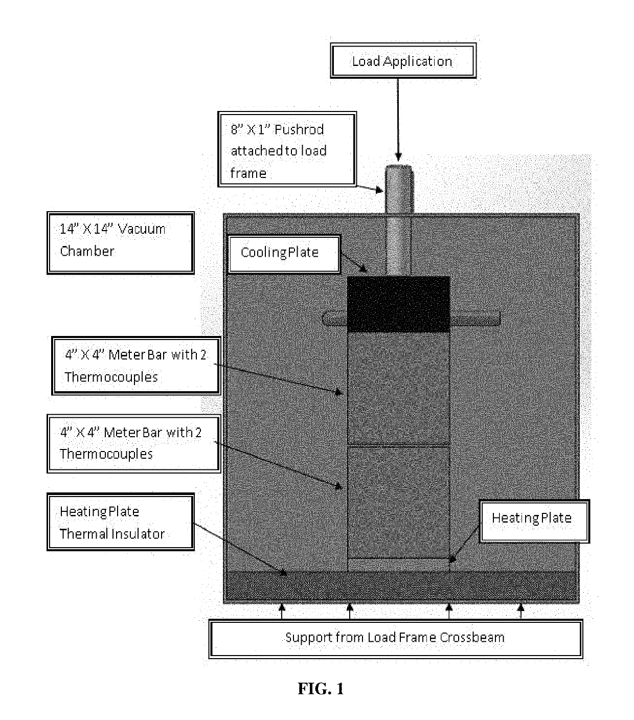
[0226]Heat transfer properties for all test specimens were evaluated using a test fixture designed and built based on the methods described in ASTM D5470 “Standard Test Method for Thermal Transmission Properties of Thermally Conductive Electrical Insulation Materials.” It not only allows for deformation of the test specimens but also incorporates a vacuum chamber to minimize conductive and convective heat losses. A schematic diagram of the fixture design is shown in FIG. 1. The vacuum chamber was constructed of stainless steel with an acrylic door, and is capable of maintaining vacuum in the 10−5 torr range. The vacuum chamber sits on the reaction plate of a 1000 lb load frame, with all feedthroughs near the top of the chamber. Thermocouples were fed via a pair of Omega 4-pair feedthroughs (8 thermocouples possible). The cooling tubes possess bulkhead fittings with o-rin...

example 2

red / Multitiered CNT-Based Thermal Interface Materials (TIMs) Containing Polymer or Adhesive

[0249]CNT arrays were grown to nominally 100 μm thickness and fully infiltrated with a soft polyurethane polymer. The thermal resistance of each individual pad was measured using a modified ASTM D570 stepped bar apparatus.

[0250]The individual samples were stacked using various methods, and the thermal resistance of the resulting stack was measured in the same manner as the single tiers.

[0251]First, two individual array samples with measured thermal resistances of 1.37 and 1.5 cm2−K / W respectively were stacked on top of one another. Solvent known to dissolve the polymer that was used to infiltrate the array was placed between the stacks to place the interface in a liquid state. The resulting stack was allowed to dry under pressure until the solvent was fully evaporated. The stack was then measured in the stepped bar system with a resulting resistance of 1.5 cm2−K / W. In this example, the thickne...

example 3

esting of Thermal Interface Materials (TIMs) Sample Fabrication of CNT-TIM Composite

[0253]Vertically aligned carbon nanotubes were grown on 50 μm 1145 H19 aluminum foil coated on both sides with an iron catalyst via low pressure chemical vapor deposition. Acetylene and hydrogen act as precursor gases and growth is performed at 630° C. in order to stay comfortably below the melting temperature of the Al substrate. CNTs are grown to two nominal heights: 15 μm (3 min growth time) or 50 μm (15 minute growth time).

[0254]It is believed that due to the difficulty of repeatably wicking a consistent thickness of bulk paraffin wax into a CNT array, while avoiding excess polymer at the tips, a powder coating technique can more reliably deliver a uniformly thin coating of wax to the CNT tips.

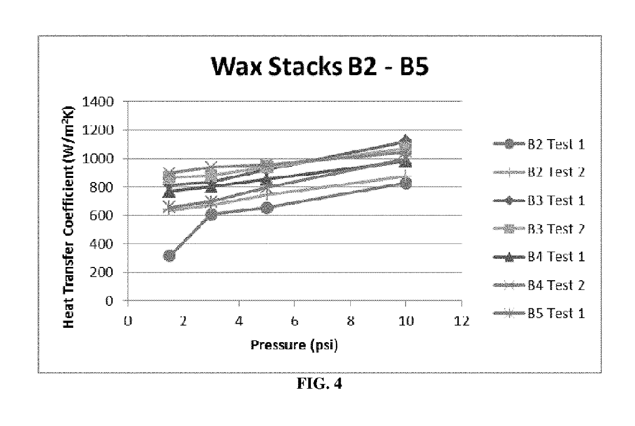
[0255]The synthetic polyethylene waxes used to powder coat the CNTs were supplied in a micronized powder form that is loaded into an Eastwood Dual Voltage HotCoat powder coating gun. Dry air at 5-8 psi was ...


PUM

PropertyMeasurementUnit
temperatureaaaaaaaaaa
pressureaaaaaaaaaa
temperatureaaaaaaaaaa

Abstract

Single-layer CNT composites and multilayered or multitiered structures formed therefrom, by stacking of vertically aligned carbon nanotube (CNT) arrays, and methods of making and using thereof are described herein. Such multilayered or multitiered structures can be used as thermal interface materials (TIMs) for a variety of applications, such as burn-in testing.

Description

CROSS-REFERENCE TO RELATED APPLICATIONS[0001]This application claims benefit of and priority to U.S. Provisional Application No. 62 / 467,649, filed on Mar. 6, 2017, which is hereby incorporated herein by reference in its entirety.FIELD OF THE INVENTION[0002]This invention is in the field of carbon nanotube arrays or sheets, particularly arrays or sheets which can be single-layered or stacked to form multilayered or multitiered structures and methods of making and using thereof.BACKGROUND OF THE INVENTION[0003]As the performance and packaging demands on modern electronics have continued to become more and more aggressive, identifying new thermal solutions has become a critical part of the design process. In nearly all thermal management applications, there are numerous heat transfer interfaces where intimate contact is needed to ensure efficient removal of heat from the package. In this space, a wide variety of thermal interface materials (TIMs) have been developed for specific applic...

Claims


Application Information

Patent Timeline
Patent Type & Authority Patents(United States)
IPC IPC(8): H01L23/373G01N25/18B82Y30/00G01R31/28C09K5/14H01L23/00H05K7/20B82Y40/00
CPCG01N25/18H01L23/3731B82Y30/00H01L24/48H05K7/20481H01L23/3735G01R31/2896C09K5/14C01B2202/24H05K2201/10151B82Y40/00H05K2201/026H01L21/4871H01L23/4928H01L22/14H01L23/373
Inventor COLA, BARATUNDEGREEN, CRAIGPRINZI, LEONARDO
Owner CARBICE CORP
Learn More