Optical materials
a technology of optical materials and materials, applied in the field of optical materials, can solve the problems of limited surface density specific to the material used for storage mediums, insufficient storage time for hdtvs (high density televisions), hard disk drives, dvd and mo,
- Summary
- Abstract
- Description
- Claims
- Application Information
AI Technical Summary
Problems solved by technology
Method used
Image
Examples
embodiment 1
[0075] Embodiment 1
[0076] Holographic storage medium
[0077] This embodiment explains an embodiment I which the present invention is applied to a holographic storage medium.
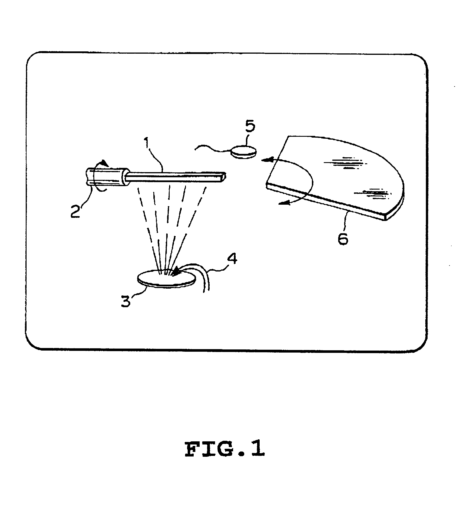
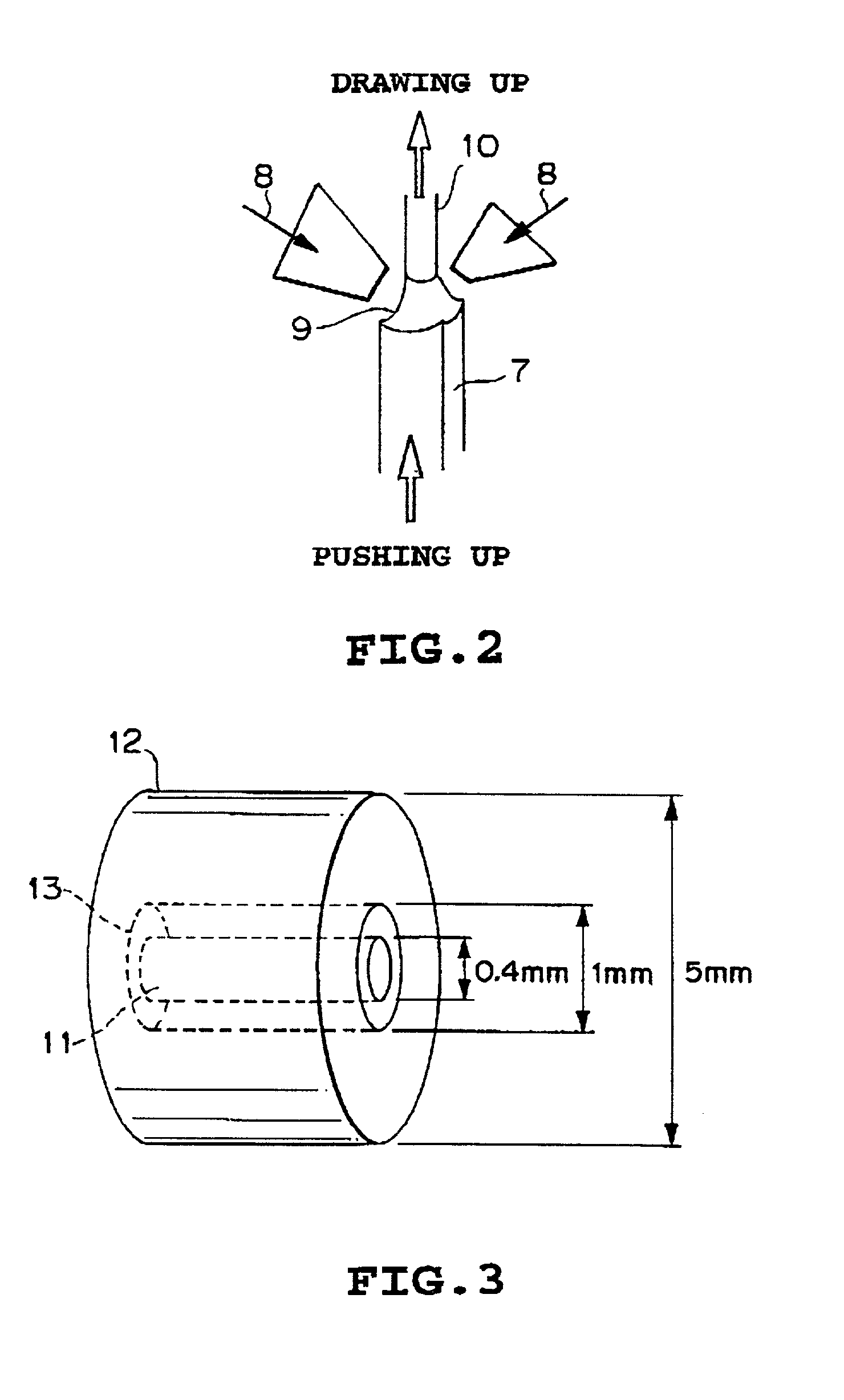
[0078] FIGS. 1 and 2 are schematic diagrams illustrating a method of producing a holographic storage medium according to an embodiment of the present invention. FIG. 1 illustrates an embodiment of a method of preparing a single crystal of strontium barium niobate (hereafter, SBN) according to the present invention, more particularly a single crystal having a composition of Sr.sub.0.61Ba.sub.0.39Nb.sub.2O.sub.6 (hereafter, "SBN.sub.61") having doped therein cerium (Ce) and europium (Eu) as impurities (hereafter, "Ce,Eu:SBN.sub.61"). First, a SBN.sub.61 single crystal containing cerium as an impurity was grown by conventional Czochralski process. Ce was charged such that 0.1% by weight based of SBN.sub.61 of CeO.sub.2 was added, which corresponded to a Ce concentration of 1.8.times.10.sup.19 cm.sup.-3. The thus obtai...
embodiment 2
[0091] Embodiment 2
[0092] Examples of lifetime and light sensitivity for various compositions
[0093] This embodiment illustrates variation of lifetime and light sensitivity depending on difference in composition.
[0094] SBN single crystals were fabricated in the same manner as in Example 1 except that the contents of Ce and Eu were 0.1% by weight and 0.01% by weight, respectively, for all the compositions with varying the amounts of Sr and Ba. Table 2 shows lifetime and light sensitivity of the resulting SBNs. Here, lifetime was expressed in terms of half-life of diffraction efficiency and light sensitivity was expressed in terms of S.eta..sup.-1. 3 S - 1= [ 1 d ( W ) ] - 1
[0095] where .eta. is diffraction efficiency, d is a length of a single crystal in the direction along which light transmits, .alpha. is absorption coefficient of light, W is a recording energy density, which is a product of light intensity and time. Evaluating by S.eta..sup.-1, the light sensitivity is higher as th...
embodiment 3
[0096] Embodiment 3
[0097] Phase Conjugate Mirror
[0098] This embodiment illustrates an embodiment in which the present invention is applied to a phase conjugate mirror.
[0099] FIG. 7 is a schematic view showing an ordinary mirror, illustrating the action of reflection of light and FIG. 8 is a schematic view showing a phase conjugate mirror according to an embodiment of the present invention, illustrating the action of reflection of light.
[0100] A plane wave 30 having a regular pattern undergo phase disturbance while transmitting through a phase disturbing object 32, such as a plastic plate having an irregular shape, air flickering due to heat, or the like and the wavefront is disturbed. When the disturbed wave 34 is input in a mirror, it behaves differently whether the mirror is an ordinary mirror or a phase conjugate mirror. As shown in FIGS. 7 and 8, when waves are reflected by an ordinary mirror 33 and a phase conjugate mirror 34, respectively, reflected waves 35 and 36 reflected b...
PUM
| Property | Measurement | Unit |
|---|---|---|
| diameter | aaaaa | aaaaa |
| wavelengths | aaaaa | aaaaa |
| thickness | aaaaa | aaaaa |
Abstract
Description
Claims
Application Information


