Photoelectric conversion element

a conversion element and photoelectric technology, applied in the direction of thermoelectric devices, electrolytic capacitors, electrochemical generators, etc., can solve the problems of -type semiconductor layer prone to penetration, solar cell not yet established as energy-saving power source, electrolyte volatilization,

Inactive Publication Date: 2002-08-15
SEIKO EPSON CORP
View PDF0 Cites 84 Cited by
  • Summary
  • Abstract
  • Description
  • Claims
  • Application Information

AI Technical Summary

Problems solved by technology

However, since these solar cells employing silicon require high manufacturing cost and a great deal of energy in manufacturing thereof, thus these solar cells are not yet established as an energy-saving power source.
H06-511113 employs an electrolyte of which vapor pressure is extremely high, there is a problem in that the electrolyte volatilizes.
However, this solar cell has a problem in that the p-type semiconductor layer is liable to penetrate the TiO.sub.2 layer to short-circuit the electrode.
The solar cell employing the CuI has a problem in that a generated current is lowered due to its deterioration caused by the increase in the crystal grain size of CuI and the like.
When a titanium alkoxide, for example, is used as the organic titanium compound, an additive such as acetic acid, acetylacetone or nitric acid is added because the titanium alkoxide is chemically unstable.
Here, if the hole transport layer material does not contain such a crystal size coarse suppressing substance, its crystal size may become too large upon crysta

Method used


Image

  • Photoelectric conversion element
  • Photoelectric conversion element
  • Photoelectric conversion element

Examples


example 1

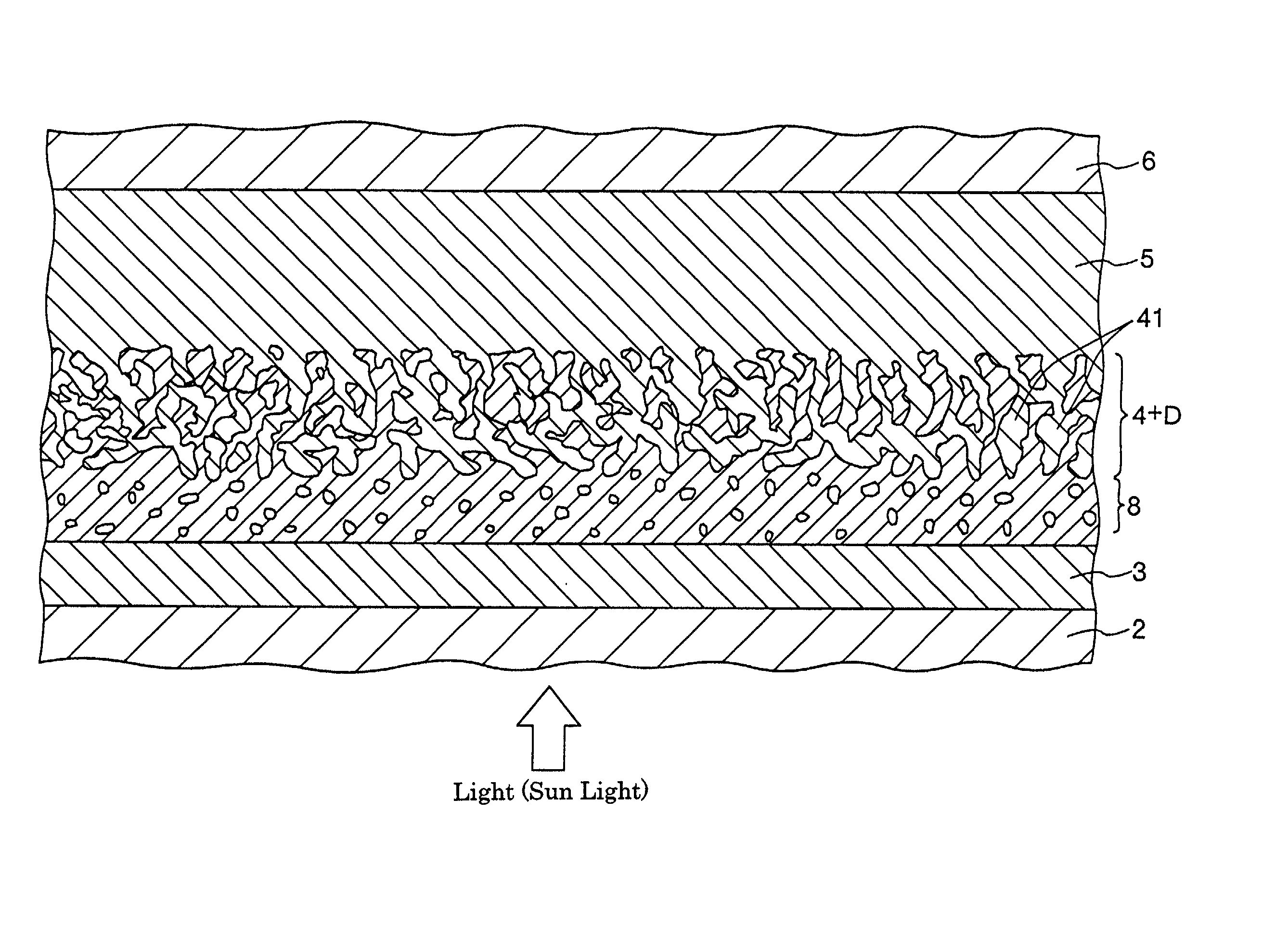
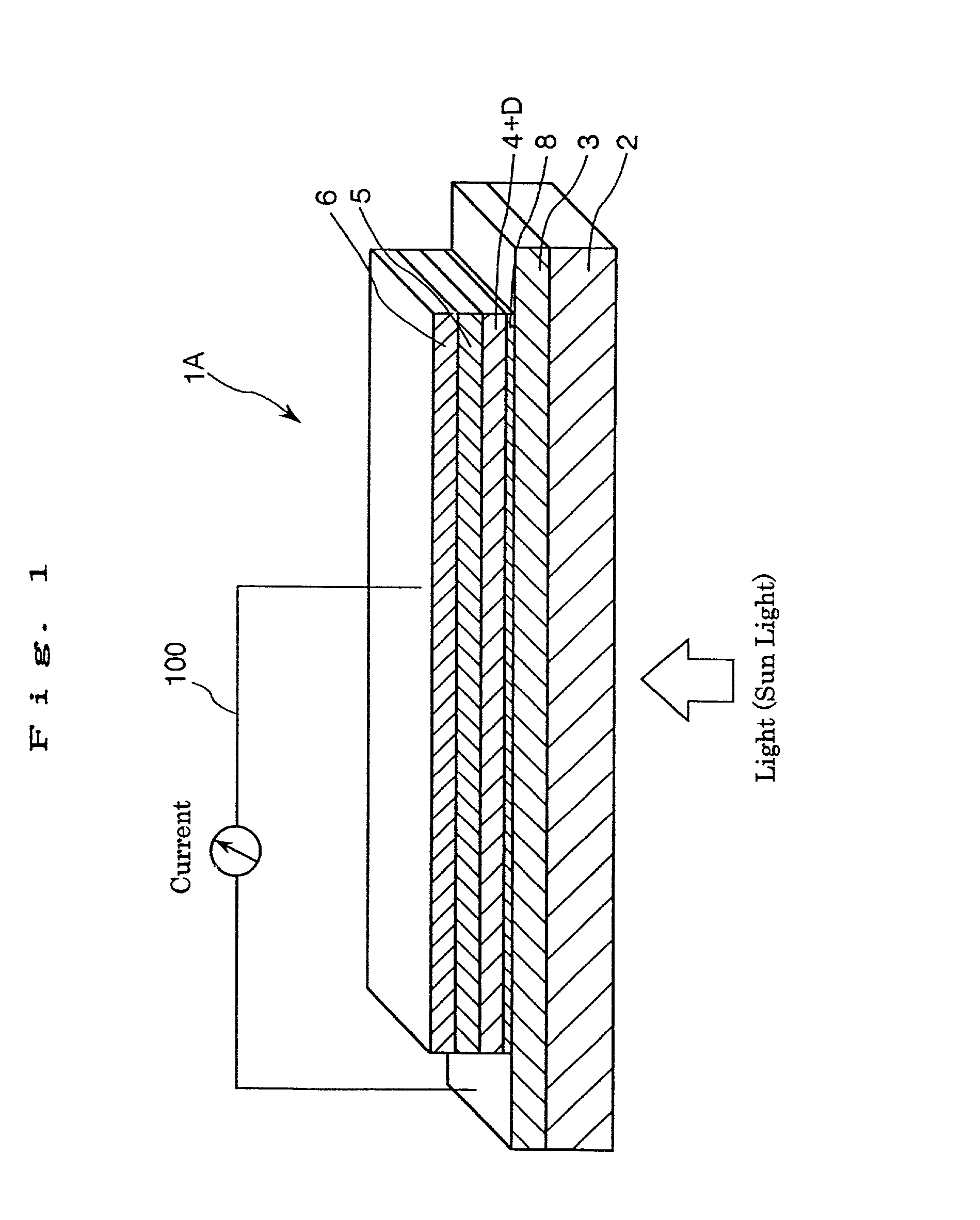
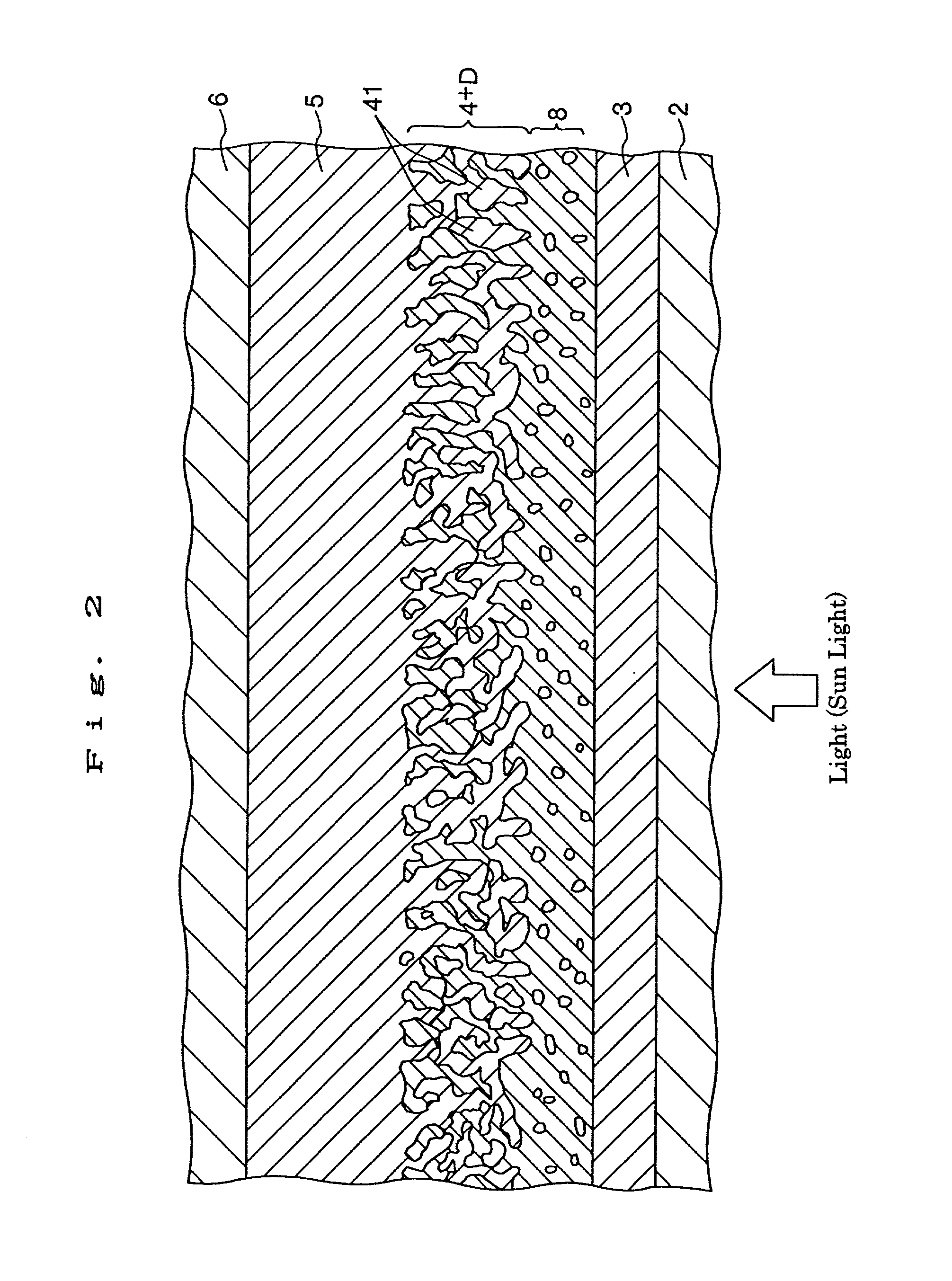
[0271] A solar cell (photoelectric conversion element) shown in FIG. 1 was manufactured as follows.

[0272] (0) First, a soda glass substrate having the size of 30 mm (length).times.35 mm (width).times.1.0 mm (thickness) was prepared. Then, this soda glass substrate was subjected to cleaning by immersing it into a cleaning solution (a mixed solution of sulfuric acid and hydrogen peroxide to clean its surface.

[0273] (1) Next, an electrode made of FTO (first electrode) having the size of 30 mm (length).times.35 mm (width).times.1.0 mm (thickness) was formed on the top surface of the soda glass substrate by means of deposition.

[0274] (2) Next, a barrier layer was formed on the region of the FTO electrode having the size of 30 mm (length).times.30 mm (width). This barrier layer was formed as follows.

[0275]

[0276] First, titanium tetraisopropoxide (organic titanium compound) was dissolved in an organic solvent of 2-n-butoxyethanol solution so that its concentration be 0.5 mol / L to obtain a...

example 2

[0302] A solar cell was manufactured in the same manner as the Example 1 excepting that the operation for forming the barrier layer was repeated twice using barrier layer materials of different compositions.

[0303]

[0304] First, titanium tetrachloride (which is an inorganic titanium compound) was dissolved in ethanol anhydride so that its concentration be 1.0 mol / L.

[0305] In this way, a barrier layer material was obtained. In this case, the viscosity of the obtained barrier layer material was 0.9 cP (at a room temperature).

[0306] Further, the porosity of the obtained barrier layer was less than 1%, and the average thickness thereof was 2.1 .mu.m.

[0307] On the other hand, the porosity of the titanium oxide layer (electron transport layer) was 35%, and the average thickness thereof was 7.4 .mu.m.

[0308] Further, the resistance value in the thickness direction of the total of the barrier layer and the titanium oxide layer was equal to or greater than 1 k.OMEGA. / cm.sup.2.

example 3

[0309] A solar cell was manufactured in the same manner as the Example 1 excepting that the operation for forming the barrier layer was repeated for three times using barrier layer materials of different compositions.

[0310]

[0311] First, titanium oxyacetonate (which is an organic titanium compound) was dissolved in 2-butanol so that its concentration be 1.5 mol / L.

[0312] In this way, a barrier layer material was obtained. In this case, the viscosity of the obtained barrier layer material was 1.3 cP (at a room temperature).

[0313] Further, the porosity of the obtained barrier layer was less than 1%, and the average thickness thereof was 3.1 .mu.m.

[0314] On the other hand, the porosity of the titanium oxide layer (electron transport layer) was 33%, and the average thickness thereof was 6.9 .mu.m.

[0315] Further, the resistance value in the thickness direction of the total of the barrier layer and the titanium oxide layer was equal to or greater than 1 k.OMEGA. / cm.sup.2.


PUM


Abstract

A solid type dye-sensitized photoelectric conversion element which is excellent in photoelectric conversion efficiency and which can be manufactured at a low cost is disclosed. The photoelectric conversion element can be applied to a so-called wet type solar cell which does not use any electrolyte. The solar cell comprises a first electrode 3, a second electrode 6 arranged opposite to the first electrode 3, an electron transport layer 4 arranged between the first electrode 3 and the second electrode 6, a dye layer D which is in contact with the electron transport layer 4, a hole transport layer 5 arranged between the electron transport layer 4 and the second electrode 6 and being in contact with the dye layer D, and a barrier layer 8, and these elements are provided on a substrate 2. The barrier layer 8 constitutes short-circuit preventing or suppressing means for preventing or suppressing short-circuit between the first electrode 3 and the hole transport layer 5. The porosity of the barrier layer is made smaller than that of the electron transport layer 4. The barrier layer is formed into a film-like shape and arranged between the fist electrode 4 and the electron transport layer 4. The solar cell can accomplish excellent photoelectric conversion efficiency by the provision of such a barrier layer 8.

Description

BACKGROND OF THE INVENTION[0001] 1. Field of the Invention[0002] The present invention relates to a photoelectric conversion element.[0003] 2. Description of the Prior Art[0004] From the approximately past ten years ago, grate attention has been paid to solar cells (photoelectric conversion element) employing silicon as a power source which is harmless to the environment. As for these solar cells employing silicon, a monocrystalline silicon type solar cell is known, which is used in artificial satellites or the like. In addition, as solar cells for practical applications, there are known a solar cell employing polycrystalline silicon (single crystal silicon) and a solar cell employing amorphous silicon. These solar cells have already been practically used in industrial and household applications.[0005] However, since these solar cells employing silicon require high manufacturing cost and a great deal of energy in manufacturing thereof, thus these solar cells are not yet established ...

Claims


Application Information

Patent Timeline
IPC IPC(8): H01G9/20H01L31/0256H01L31/04H01L31/042H01L31/06H01L51/30H01M14/00
CPCH01G9/2031H01L51/0084H01L51/4226Y02E10/542Y02E10/549H10K85/341H10K30/151H10K30/50H01L31/04H01M14/00
Inventor FUJIMORI, YUJIMIYAMOTO, TSUTOMU
Owner SEIKO EPSON CORP
Why Eureka
Try Eureka