Semiconductor manufacturing apparatus

a manufacturing apparatus and semiconductor technology, applied in the direction of coatings, chemical vapor deposition coatings, electric discharge tubes, etc., can solve the problems of deterioration of semiconductor device properties, acceleration of device property deterioration, and increase of consumption power

Inactive Publication Date: 2002-08-15
TOKYO ELECTRON LTD
View PDF0 Cites 36 Cited by
  • Summary
  • Abstract
  • Description
  • Claims
  • Application Information

AI Technical Summary

Benefits of technology

[0016] The other object of the present invention is to provide a method and an apparatus for manufacturing semiconductors that can form a SiN film of high quality in a short time.
[0020] In addition, in the present manufacturing method, a process for forming, due to direct nitriding or oxidizing or oxy-nitriding, an insulator film of good quality at an interface with the silicon substrate and a process for forming thereon, due to CVD method, the rest of the insulator film can be independently implemented. Accordingly, compared with the case where all process is implemented by direct nitriding only or CVD method only to form an insulator film, the film quality at the interface with the silicon substrate can be improved in regulation to result in an insulator film of better quality.
[0026] According to the present method, in an atmosphere of a processing gas, on an object to be processed consisting mainly of silicon, microwaves are irradiated through a planar-array antenna having a plurality of slits, so-called RLSA (Radial Line Slot Antenna) antenna. Thereby, the plasma is directly supplied on the silicon substrate to form a SiN insulator film. Accordingly, film quality at the interface with SiN insulator film formed on a surface of the silicon substrate can be successfully regulated.
[0027] Furthermore, according to another manufacturing method of the present invention, on a first insulator film formed by use of so-called RLSA antenna, all the second insulator film can be formed by irradiation of the plasma of low damage. As a result of this, a SiN film of high quality can be formed. In particular, when the second insulator film is formed by use of the CVD method, the insulator film can be deposited in a short time to result in formation of a SiN film of high equality in a short time.
[0029] Therefore, a silicon nitride film (SiN film) that does not cause a large leakage current when thinning down to approximate 40 angstroms is being considered to use as a gate insulator.
[0035] The present invention is made under such circumstances. An object is to provide a method for manufacturing semiconductor devices provided with an insulator film of excellent electrical property and of higher deposition rate.

Problems solved by technology

However, when the SiO.sub.2 layer is 4 .mu.m or less, a leakage current (gate leakage current) flowing the gate insulator increases to cause problems such as an increase of consumption power or an acceleration of deterioration of device property.
In addition, there is such a problem that during formation of a gate electrode, boron contained therein causes alloy spikes in the SiO.sub.2 film to reach the silicon substrate to result in deterioration of semiconductor device property.
When the SiN films are deposited by use of CVD method, there occur many incomplete bonds (dangling bond) at the interface with the silicon substrate to result in deterioration of device property.
The dopant diffuses differentially to cause deterioration of device property.
However, in the case of depositing SiN layers with the plasma, the following problems have been pointed out.
That is, ions in the plasma are accelerated by a plasma sheath voltage to bombard the silicon substrate with high energy, thereby so-called plasma damage occurs at interfaces of the silicon substrate or on the silicon substrate to deteriorate the device property.
However, even when silicon nitride is formed with this plasma device, in the case of forming SiN films by use of direct nitriding method, there is the following problem.
That is, in order to obtain interfaces of good quality of less dangling bond defects by dominantly distributing oxygen only at the interfaces of the silicon substrate, there is a difficulty in regulating film quality at the interfaces with the silicon substrate.
That is a slow process to require a long time to give prescribed processing to an object being processed.
Accordingly, the objects can not be processed much per unit period to cause difficulties in industrial application.
When tried to make thinner than this, a leakage current becomes larger to result in larger power consumption.
This is impractical.
However, silicon nitride film due to thermal nitriding has a lot of dangling bonds (free species) and is poor in electrical properties.
Silicon nitride film (silicon nitride film) due to low-pressure vapor phase growth method also is poor in electrical properties.
In addition, silicon oxynitride film takes a long time to form.
Although SiN film of excellent electrical property can be obtained by this means, there is a disadvantage that SiN film can not be formed with a high rate.

Method used


Image

  • Semiconductor manufacturing apparatus
  • Semiconductor manufacturing apparatus
  • Semiconductor manufacturing apparatus

Examples


embodiment

[0107] (Embodiment)

[0108] In the following, embodiment will be shown.

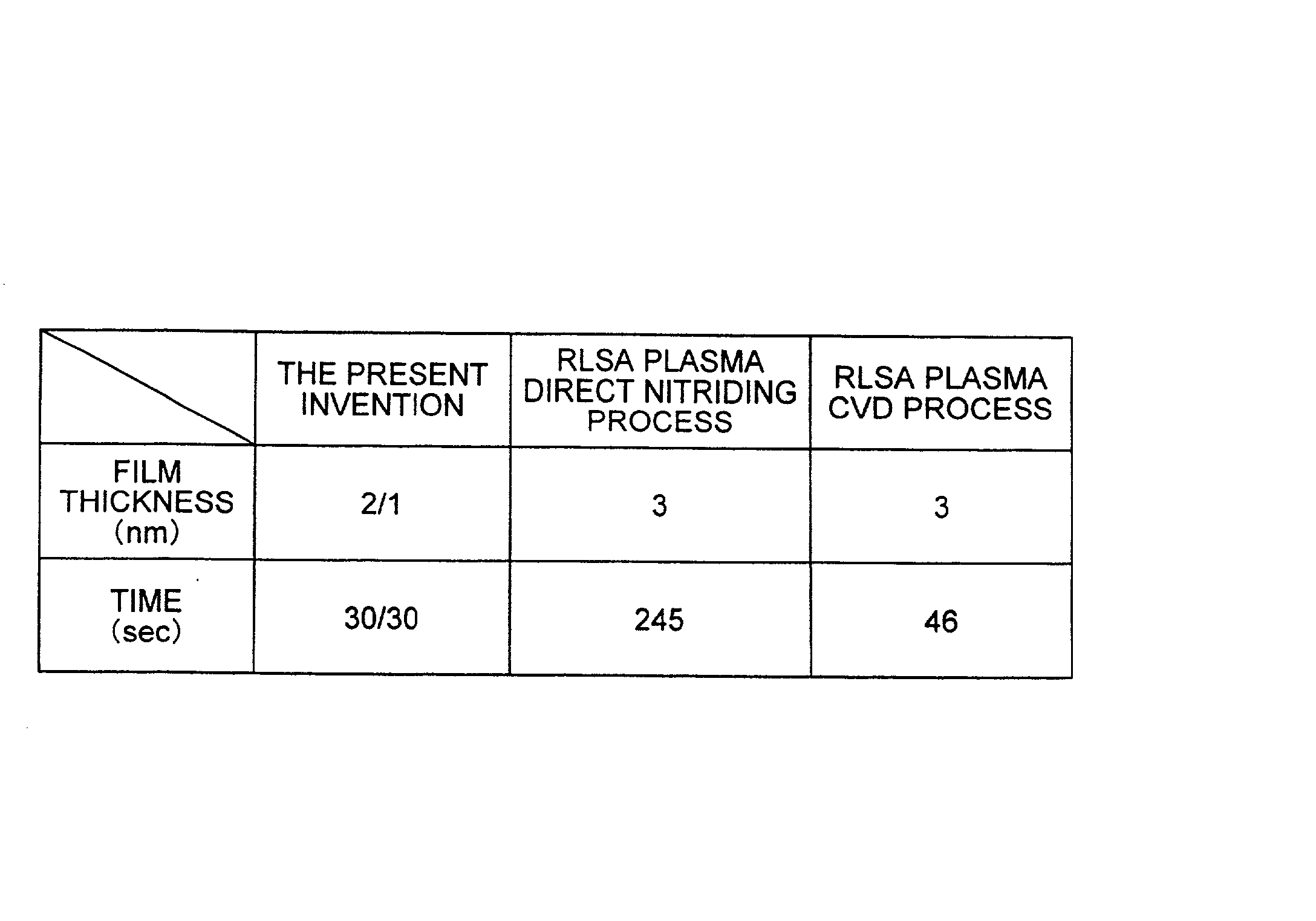
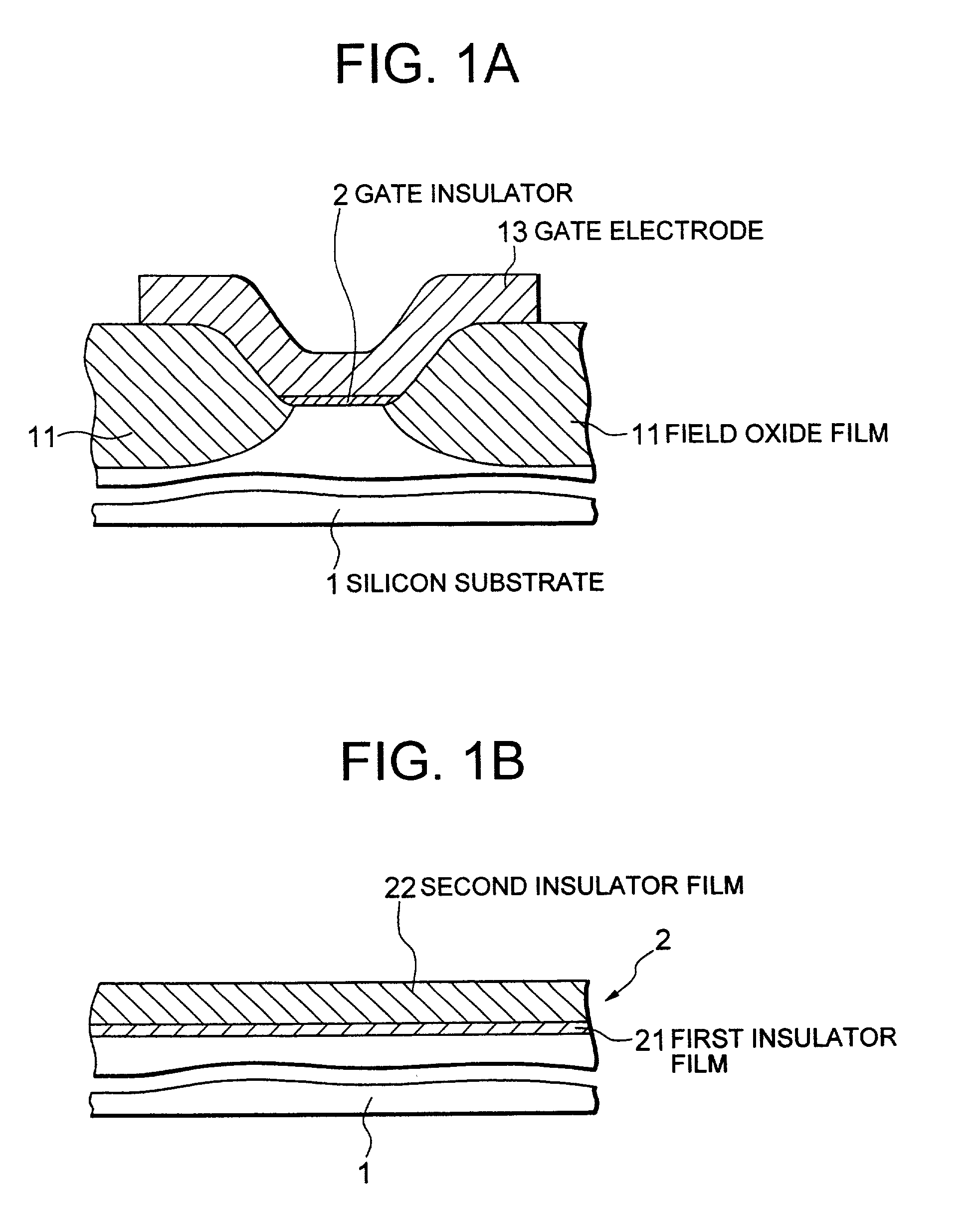
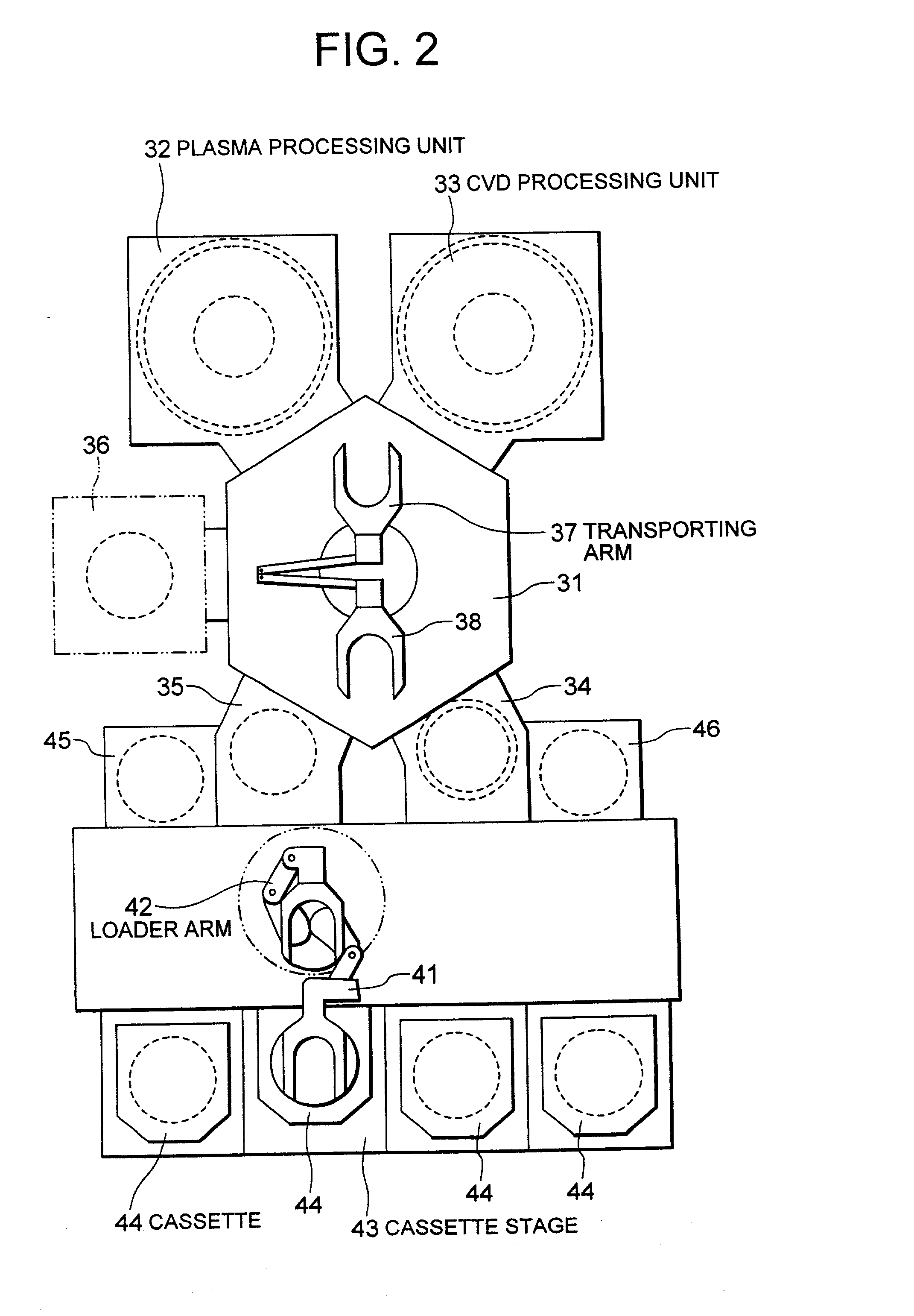
[0109] According to the present manufacturing method of semiconductors, on an n type silicon substrate in which device isolation is implemented, with an apparatus as shown in FIG. 2, with RLSA plasma, at a processing unit 32 shown in FIG. 2, a SiON film of 2 nm thickness is deposited. The total thickness of the insulator film is 3 nm (in terms of oxide film thickness). The SiON film is deposited under conditions of the flow rates of Xe / N.sub.2 / H.sub.2 / O.sub.2=500 sccm / 25 sccm / 15 sccm / 1 sccm, a pressure of 100 mTorr, microwave output power of 2.0 kW, and a temperature of 400.degree. C.

[0110] The CVD deposition is carried out under the conditions of the flow rates of Xe / SiH.sub.4 / N.sub.2=500 sccm / 15 sccm / 20 sccm, a pressure of 100 mTorr, microwave power of 25 kW and a temperature of 400.degree. C. The deposition time is 62 sec. Under these conditions, throughput of 40 pieces / hour is attained and practical applicabili...


PUM

PropertyMeasurementUnit
thicknessaaaaaaaaaa
temperatureaaaaaaaaaa
plasma sheath voltageaaaaaaaaaa

Abstract

In an atmosphere of processing gas, on a wafer W consisting mainly of silicon, through a planar-array antenna RLSA 60 having a plurality of slits, microwaves are irradiated to generate plasma containing oxygen, or nitrogen, or oxygen and nitrogen and to implement therewith on the surface of the wafer W direct oxidizing, nitriding, or oxy-nitriding to deposit an insulator film 2 of a thickness of 1 nm or less in terms of oxide film. A manufacturing method and apparatus of semiconductors that can successfully regulate film quality of the interface between a silicon substrate and a SiN film and can form SiN film of high quality in a short time can be obtained.

Description

[0001] 1. Field of the Invention[0002] The present invention relates to a manufacturing method of semiconductors, in particular detail, to a method for forming gate insulators in MIS (MOS) semiconductor devices, and to a manufacturing method of semiconductor devices provided with insulator films such as gate insulators on a surface of a silicon substrate.[0003] 2. Description of the Related Art[0004] Recently, as MIS (MOS) semiconductors have been patterned finer, extremely thin gate insulators such as approximately 4 nm or less are in demand. So far, for gate insulator material, silicon oxide films (SiO.sub.2 film) have been industrially used that can be obtained by directly oxidizing a silicon substrate by use of a high temperature furnace of approximately 850.degree. C. to 1000.degree. C.[0005] However, when the SiO.sub.2 layer is 4 .mu.m or less, a leakage current (gate leakage current) flowing the gate insulator increases to cause problems such as an increase of consumption pow...

Claims


Application Information

Patent Timeline
Patent Type & Authority Applications(United States)
IPC IPC(8): H01L21/314H01L21/316H01L21/318
CPCH01J37/32192H01L21/0214H01L21/0217H01L21/022H01L21/02211H01L21/02238H01L21/02249H01L21/02252H01L21/02255H01L21/02274H01L21/02332H01L21/02337H01L21/3144H01L21/31662H01L21/3185
Inventor KAWAKAMI, SATORUMURAKAWA, SHIGEMIYUASA, MITSUHIROHONGOH, TOSHIAKI
Owner TOKYO ELECTRON LTD
Why Eureka
Try Eureka