
Solder jointing system, solder jointing method, semiconductor device manufacturing method, and semiconductor device manufacturing system

a solder jointing and solder jointing technology, applied in the direction of muffle furnaces, lighting and heating apparatus, furnaces, etc., can solve the problems of increasing the fabrication cost, bringing about the explosion of the solder jointing atmosphere, and the desired solder jointing method that does not need cleaning, so as to reduce the ability and improve the safety of the cleaning process.

Inactive Publication Date: 2002-09-19
SOCIONEXT INC
View PDF0 Cites 57 Cited by
  • Summary
  • Abstract
  • Description
  • Claims
  • Application Information

AI Technical Summary

Benefits of technology

[0058] The present invention has been made in light of the above problems, and it is an object of the present invention to provide a solder jointing system which is capable of having a high processing capability and capable of preventing the re-oxidation or eliminating the danger of the explosion.
[0059] It is another object of the present invention to provide a solder jointing system and a solder jointing method which is capable of improving the throughput of the solder joint rather than the prior art, or preventing the generation of the residue on the substrate after the solder joint.
[0060] It is still another object of the present invention to provide a semiconductor device manufacturing method and a semiconductor device manufacturing system that is capable of removing uniformly and effectively the surface oxide film formed on the surface of the electrode or the wiring that contains the copper as the major material.

Problems solved by technology

In this case, since the dissolved product cannot be simply removed by the organic solvent not-containing flon or trichlene in this cleaning, a large quantity of organic solvent must be used in this cleaning.
However, since the organic solvent exerts a harmful influence upon the environment, the development of the solder jointing method that does not need the cleaning is desired.
Therefore, the thorough cleaning is needed, which acts as the cause to bring about the increase of the fabrication cost.
First, the first subject is that the danger of the explosion in the solder jointing atmosphere is present.
However, the diketone is such material that is expensive as set forth in the literature 3 and has the danger of the explosion.
If the temperature and the concentration in the processing layer and the oxygen concentration exceed respective certain ranges, e.g., if the formic acid concentration and the oxygen concentration reach 30% and 10% at the temperature of 100.degree. C. respectively, there exists the danger of the explosion.
The equipment and the method that have the possibility to reach such conditions causing the danger of the explosion are not readily accepted.
However, the solder joint in the chamber has small processing capability.
Since the substrate is loaded / unloaded one by one into / from the solder jointing system, i.e., such solder jointing system has the so-called sheet-fed processing structure, efficiency of the solder joint is low.
In this case, since this equipment is substantially equivalent to the employment of a plurality of solder jointing systems, not only the cost is increased but also the wide area is needed.
It is difficult to use the strong acid or the alkaline as the chemicals since the underlying wiring made of the copper is exposed in the via hole, so that the weak-acid cleaning is often employed.
Since this copper oxide is inferior in conductivity, it is executed usually to remove such copper oxide by executing the cleaning process.
However, there are the problems described hereunder in the above cleaning methods in the prior art.
However, there is the problem that the corrosion of the copper wiring, etc. is generated in the course during when the PH value of the chemicals is being changed from the acid to the neutral.
Also, if a large quantity of dissolved oxygen is also present in the chemicals, the corrosion proceeds locally.
Therefore, in the cleaning method in the prior art, there is the problem that the uniform etching cannot be achieved.
Therefore, there is the problem that the formation of the fine buried electrode cannot be achieved.
In this case, since the copper wiring, etc. are exposed to the atmosphere in the period from the CMP to the deposition of the CVD film, the oxidation of the copper wiring, etc. is unavoidable.
Therefore, there is the problem that the coverage of the CVD film is locally degraded.
But the cleaning action of this method is not sufficient.
Therefore, there is the problem that the effective cleaning cannot be executed.
However, if the joint material whose resistivity is totally different from the electrode material is employed in transmitting the high speed signal, the reflection of the electromagnetic field is generated at that portion to disturb the high speed transmission.

Method used


Image

  • Solder jointing system, solder jointing method, semiconductor device manufacturing method, and semiconductor device manufacturing system
  • Solder jointing system, solder jointing method, semiconductor device manufacturing method, and semiconductor device manufacturing system
  • Solder jointing system, solder jointing method, semiconductor device manufacturing method, and semiconductor device manufacturing system

Examples


first embodiment

[0131] (First Embodiment)

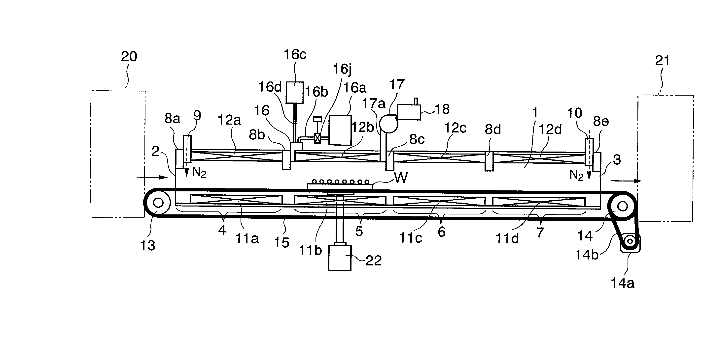
[0132] FIG. 1 is a sectional view showing a solder jointing system according to a first embodiment of the present invention.

[0133] In FIG. 1, a chamber 1 has a loading port 2 for taking a solder-adhered object (work) w such as the semiconductor device, the electronic parts, or the like into the inside and an unloading port 3 for taking out the solder-adhered object w to the outside. Both the loading port 2 and the unloading port 3 are opened into the air.

[0134] First to fourth areas 4 to 7 are arranged in sequence from the loading port 2 to the unloading port 3 in the chamber 1. The first to fourth areas (spaces) 4 to 7 have a size in which the solder-adhered object w can be placed respectively, and they are partitioned longitudinally by gas shielding plates 8a to 8e with a heater, which are fitted to the upper portion of the chamber 1.

[0135] In the chamber 1, inert gas introducing pipes 9, 10 for discharging the inert gas such as nitrogen, argon, or the lik...

second embodiment

[0178] (Second Embodiment)

[0179] In the first embodiment, one exhaust fan 17 is connected only to the second area 5 in the chamber 1. In addition to this, as shown in FIG. 10, sucking pipes 23a, 24a, 25a of exhaust fans 23, 24, 25 may be provided near the boundary portion between the first area 4 and the second area 5, near the boundary portion between the third area 6 and the fourth area 7, and near the unloading port 3 in the fourth area 7 respectively. The formic-acid recovering mechanism 18 having the same structure is fitted to exhaust ports of these exhaust fans 23, 24, 25.

[0180] If the exhaust fans 17, 23, 24, 25 are provided to the first area 4 to the fourth area 7 respectively, the atmosphere of the second area 5 can be set easily to the constant low pressure state by adjusting the pressure in the first area 4, the third area 6, and the fourth area 7 one by one. For example, if the exhaust of the exhaust fans 17, 24 in the second area 5 and the third area 6 is set stronger ...

third embodiment

[0183] (Third Embodiment)

[0184] In the first embodiment, the gas shielding plates 8b to 8d are provided to the boundaries between the first area 4 and the second area 5, the second area 5 and the third area 6, and the third area 6 and the fourth area 7 respectively. In this case, as shown in FIGS. 12A and 12B, the air curtain may be provided instead of the gas shielding plates 8b, 8c provided before and after the second area 5.

[0185] In FIGS. 12A and 12B, nitrogen-gas supplying mechanisms 26a, 26b are provided before and after the second area 5 in the chamber 1 in place of the gas shielding plates 8b, 8c, and also gas sucking / recovering mechanisms 27a, 27b are fitted to positions, that oppose to the nitrogen-gas supplying mechanisms 26a, 26b and are below the conveyer belts 15, respectively.

[0186] The nitrogen-gas supplying mechanisms 26a, 26b inject the nitrogen gas, which is fed from an external nitrogen supply source, downward into the chamber 1. The nitrogen gas discharged from ...


PUM

PropertyMeasurementUnit
Pressureaaaaaaaaaa
Pressureaaaaaaaaaa
Pressureaaaaaaaaaa

Abstract

There are provided a chamber having openings which are opened to an outer air and through which a solder-adhered object w is passed and having a heating / melting area and carrying areas arranged adjacent to the heating / melting area, a carrying mechanism for carrying the solder-adhered object w into the heating / melting area, a formic-acid supplying means for supplying a formic acid into the heating / melting area, an exhausting means for exhausting a gas from the heating / melting area and its neighboring area to lower a pressure in the heating / melting area rather than an outer air, heating means for heating directly or indirectly the solder-adhered object w in the heating / melting area, and air-stream suppressing means for disturbing a gas flow between the heating / melting area and the carrying areas. Accordingly, there can be provided a solder jointing system for jointing solder layers of the semiconductor device, the electronic device, or the like to the wirings or the pads, which is capable of having a high processing ability and preventing re-oxidation.

Description

CROSS-REFERENCE TO RELATED APPLICATIONS[0001] This application is based upon and claims priority of Japanese Patent Applications No.2001-10423, filed in Jan. 18, 2001, and 2001-172960, filed in Jun. 7, 2001, and No. 2001-67615, filed in Mar. 9, 2001, the contents being incorporated herein by reference.BACKGROUND OF THE INVENTION[0002] 1. Field of the Invention[0003] The present invention relates to a solder jointing system and a solder jointing method and, more particularly, a solder jointing system and a solder jointing method employed to joint the solder layer to wirings or pads of the semiconductor device or the electronic device.[0004] The present invention relates to a semiconductor device manufacturing method and a semiconductor device manufacturing system and, more particularly, a semiconductor device manufacturing method and a semiconductor device manufacturing system having a step / means for removing unnecessary substance that is adhered onto a surface of the electrode or th...

Claims


Application Information

Patent Timeline
IPC IPC(8): B23K1/012B23K1/008H01L21/60H05K3/34
CPCB23K1/008B23K2101/36H05K3/3489B23K1/012
Inventor MATSUKI, HIROHISAMATSUI, HIROYUKIYOSHIDA, EIJIOHNO, TAKAOOTAKE, KOKIMIZUTANI, AKIYOMIYAJIMA, MOTOSHUMIZUKOSHI, MASATAKAWATANABE, EIJI
Owner SOCIONEXT INC
Learn More