

Reflection type liquid crystal display device and manufacturing method thereof
a liquid crystal display device and reflection film technology, applied in optics, instruments, electrical devices, etc., can solve the problems of reducing power consumption, changing the film quality of reflection film, and complicated process
- Summary
- Abstract
- Description
- Claims
- Application Information
AI Technical Summary
Benefits of technology
Problems solved by technology
Method used
Image

Examples
fabrication example 7
[0296] Resist AFP 750 is coated on a 0.7 mm thick glass substrate to be a 3 .mu.m thickness, baked for 30 minutes at 90.degree. C., and UV was irradiated at 32 mJ / cm.sup.2 using a mask where circular patterns with a 10 .mu.m diameter are arranged at random. After UV irradiation, the resist film was soaked in MF 319 developer so as to form circular patterns. After baking the substrate for 40 minutes at 120.degree. C. to completely evaporate the developer in the resist, UV was irradiated at 1300 mJ / cm.sup.2 and 2600 mJ / cm.sup.2. Then the resist was baked for one hour at 200.degree. C. so as to form undulation.
[0297] FIG. 79 shows a micro-photograph of a patterned resist substrate after baking. As the photograph shows, fine wrinkled undulation is generated on the circular patterns by UV irradiation. However it was discovered that fine undulation is not generated when the same experiment was performed by increasing the UV dose to 80 mJ / cm.sup.2 to form circular patterns.
[0298] So we exa...
fabrication example 8
[0300] As FIG. 81 shows, striped undulation 303 (height: 0.5 .mu.m, width: 15 .mu.m) were formed on the glass substrate 301, and resist layer 304 (AFP 750) was coated thereon. After baking for 30 minutes at 90.degree. C., UV at 3900 mJ / cm.sup.2 was irradiated, and the resist was baked for one hour at 200.degree. C.
[0301] FIG. 82 shows micro-photographs of fine micro-groove shapes which are generated after baking.
[0302] For comparison, FIG. 82 also shows a micro-photograph of a fine micro-groove shape when undulation is not formed under the resist film. When undulation exist under the resist film, a step difference is formed on the surface of the resist, where the stress applied inside the resist differs, so the fine micro-groove shape becomes different from the peripheral area.
[0303] As described above, according to the present embodiment, a simplification of process, improvement of yield and a decrease in manufacturing cost can be implemented, and a reflection liquid crystal displa...
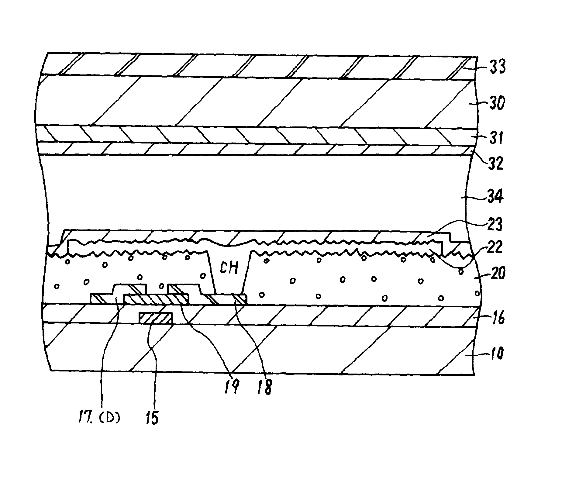
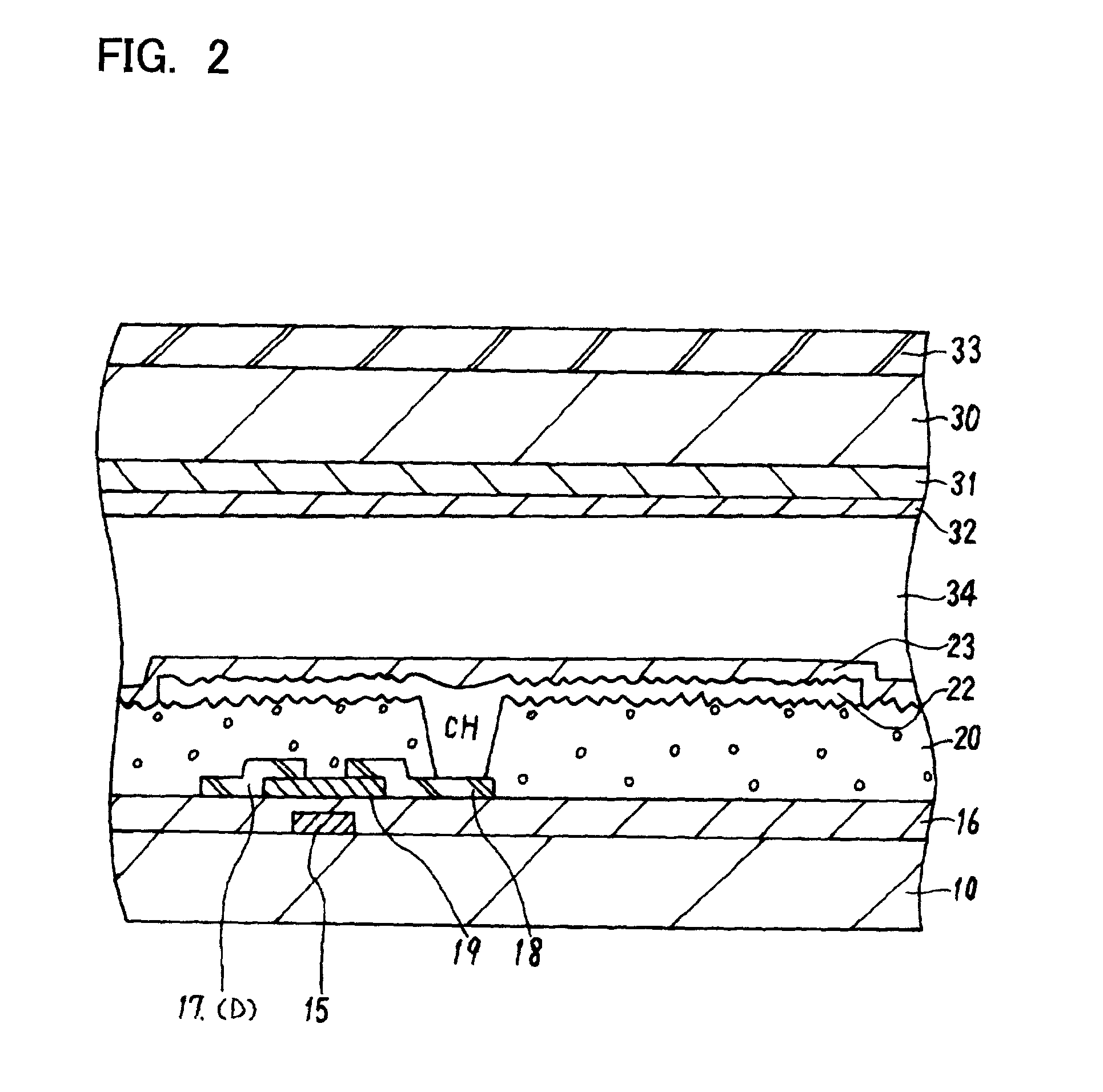
fabrication example 1
[0449] FIG. 90 is a cross-sectional view depicting a rough configuration of the reflection type liquid crystal display device of the fabrication example 1. This example has the above mentioned first feature where 501 is a cold cathode tube, 502 is a reflector, 503 is a light guiding plate, 504 is a circular polarizer, 505 is a reflection type liquid crystal panel, and 506 is a low refractive index layer.
[0450] The light guiding plate 503 is fabricated by press-molding acrylic resin with refractive index n=1.49. The surface of the light guiding plate 503 is comprised of a first inclined face 503B, which rises from a flat plane, or from a plane in parallel with the flat plane at a first angle, and a second inclined face 503A, which is adjacent to the first inclined face 503B, and which falls at a second angle which is larger than the first angle. As FIG. 90 shows, the incident face 503D and the plane 503C (the above mentioned flat plane) are almost perpendicular to each other, the pla...
PUM
 Abstract
Description
Claims
Application Information