Polysilicon doped transistor using silicon-on-insulator and double silicon-on-insulator

a polysilicon and transistor technology, applied in transistors, electrical devices, semiconductor devices, etc., can solve the problems of reducing the active device dimension, limiting the performance which can be obtained, and difficulty in scaling semiconductor structures

Inactive Publication Date: 2002-11-21
GOOGLE LLC
View PDF0 Cites 5 Cited by
  • Summary
  • Abstract
  • Description
  • Claims
  • Application Information

AI Technical Summary

Problems solved by technology

However, while some structures can be formed at such small sizes, others cannot and adjustments in operating parameters are often required.
In other cases, difficulty in scaling semiconductor structures when seeking to exploit newly developed lithographic capabilities may be the principal limiting factor in the successful reduction of active device dimensions or limit the performance which can be obtained from an active device of a given size at the limit of lithographic resolution.
Some active device structures simply do not scale well to smaller sizes.
This problem led to the development of lightly doped drain structures, now more generally referred to as extension implants since optimal impurity concentrations can be substantial while the dimensions thereof are generally very small.
Also, gate to substrate capacitance has limited performance and led to so-called "halo" implants to increase the impurity concentration grad...

Method used


Image

  • Polysilicon doped transistor using silicon-on-insulator and double silicon-on-insulator
  • Polysilicon doped transistor using silicon-on-insulator and double silicon-on-insulator
  • Polysilicon doped transistor using silicon-on-insulator and double silicon-on-insulator

Examples


Embodiment Construction

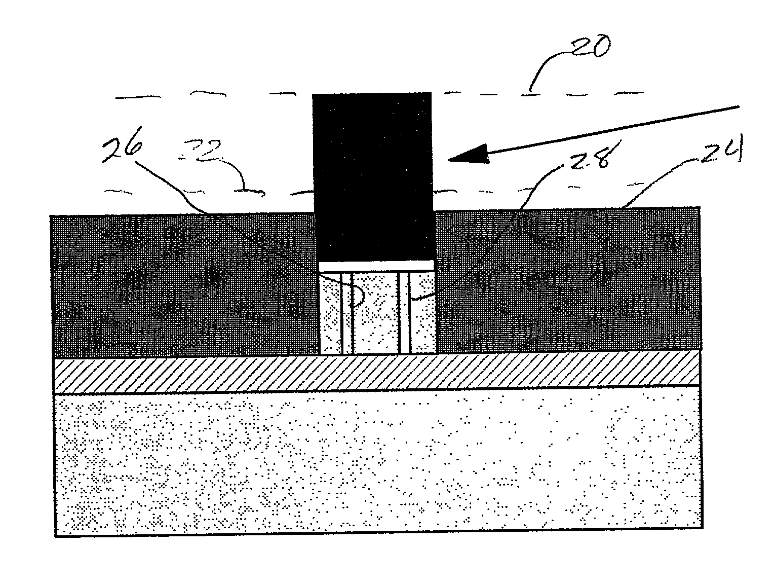
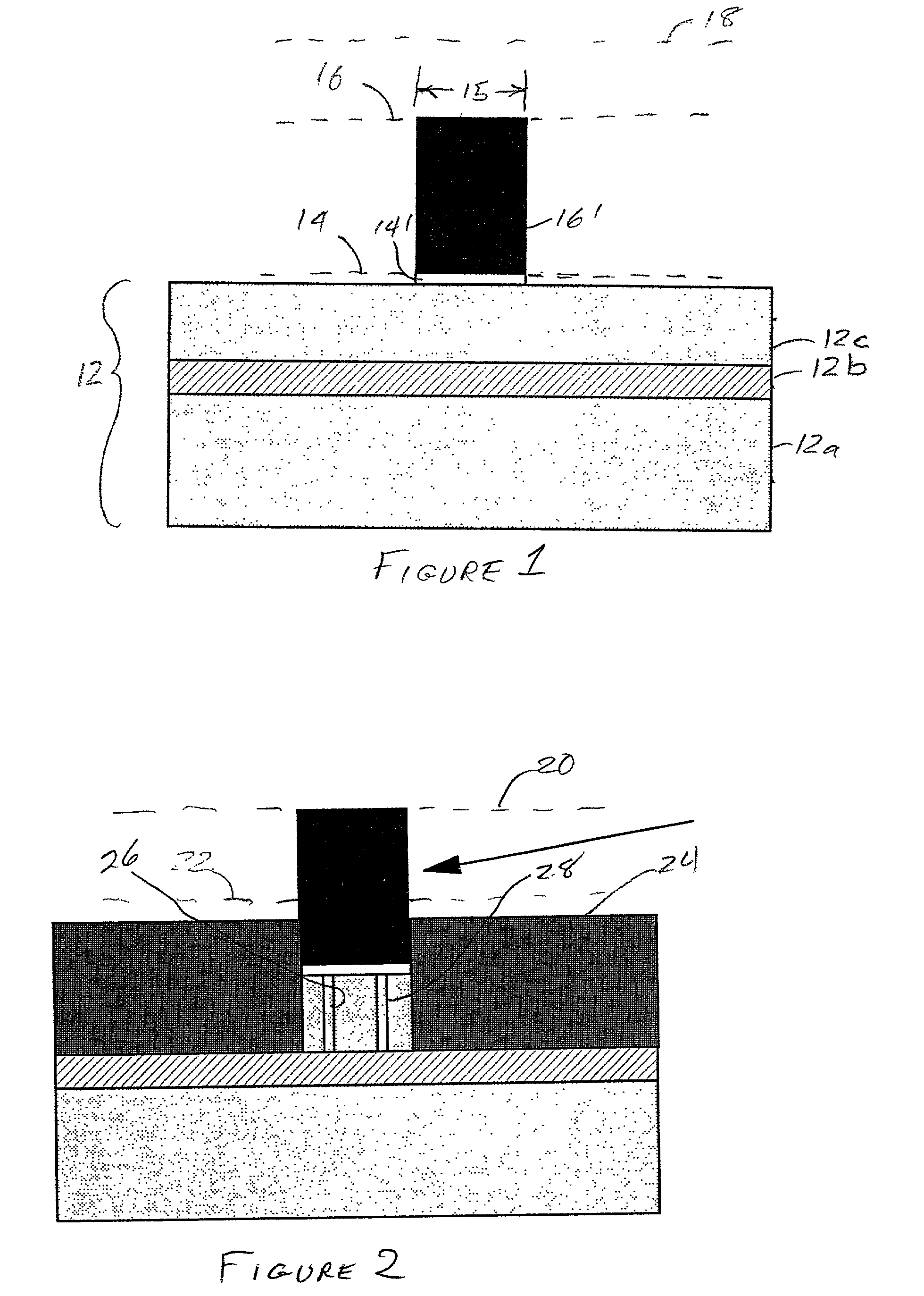
[0023] Referring now to the drawings, and more particularly to FIG. 1, there is shown, in cross-sectional view, an initial stage in the fabrication of a field effect transistor in accordance with the invention. It should be understood that while the invention will be described assuming SOI and double SOI technology, as is currently considered to be preferred for some applications, it is also applicable to other semiconductor materials such as germanium and Group III-V materials and combinations or alloys thereof such as SiGe on insulator. It should also be understood that layer 12 is a composite of three layers depicted as a bulk material or handling substrate 12a, a bottom or buried oxide (or other insulator) layer 12b and an SOI layer 12c.

[0024] A thin pad oxide layer 14 is deposited or grown to a thickness of about 8 nm on SOI layer 12c. This pad oxide could be left in the device as a gate oxide but it is preferred to later remove and reform it to increase reliability, uniformity...


PUM


Abstract

Steep concentration gradients are achieved in semiconductor device of small sizes formed on SOI or double SOI wafers by using implanted polycrystalline material such as polysilicon as a solid diffusion source. Rapid diffusion of impurities along grain boundaries relative to diffusion rates in monocrystalline materials provides a substantially constant impurity concentration at the interface between polycrystalline material and monocrystalline material. Steepness of the impurity concentration gradient is thus effectively scaled as transistor size is decreased to counter increased short channel and other deleterious effects. In the case of SOI wafers greater uniformity of electrical characteristics are achieved using the high quality of semiconductor material made available therein consistent with the relatively thin active layer. In the case of double SOI, a ground plane is formed under the conduction channel which regulates the geometry of the electric field in the conduction channel with much the same functional improvements as is achieved in dual gate transistor designs.

Description

[0001] 1. Field of the Invention[0002] The present invention generally relates to Field effect transistors suitable for use in high density integrated circuits and, more particularly, to field effect transistors of extremely small size with reduced short channel effects formed on silicon-on-insulator (SOI) and double SOI substrates.[0003] 2. Description of the Prior Art[0004] The potential for increased performance and functionality of integrated circuits by increased proximity of devices has provided a strong incentive to increase integration density to decrease length of signal propagation paths, and increase the number of devices which can be formed on a single chip of a given size. Reduction of signal path length reduces interconnection resistance and capacitance and allows reduction of signal propagation time as well as susceptibility to capacitive or inductive coupling of noise. Such reductions in interconnect capacitance must also be accompanied by reductions in device dimens...

Claims


Application Information

Patent Timeline
IPC IPC(8): H01L21/336H01L29/786
CPCH01L29/66757H01L29/66772H01L29/78654H01L29/78621H01L29/78648H01L29/78618
Inventor MULLER, K. PAULSCHEPIS, DOMINIC J.SHAHIDI, GHAVAM G.
Owner GOOGLE LLC
Why Eureka
Try Eureka