Method for producing multilayer substrate and electronic part, and multilayer electronic part

a technology of electronic parts and substrates, applied in the direction of conductive pattern formation, fixed capacitors, stacked capacitors, etc., can solve the problems of reducing the thickness of the substra

Inactive Publication Date: 2003-02-13
TDK CORPARATION
View PDF1 Cites 50 Cited by
  • Summary
  • Abstract
  • Description
  • Claims
  • Application Information

AI Technical Summary

Benefits of technology

0013] An object of the present invention is to provide a method for producing a multilayer substrate or an electronic part as well as multilayer e

Problems solved by technology

The use of sintered ferrite and sintered ceramics, however, gives rise to several problems.
Sintered materials suffer from inherent defects including cracks and warp caused by firing.
Cracks are also induced by the differential thermal expansion between sintered material and printed circuit board.
With resinous materials as such, however, a satisfactory dielectric constant is arrived at with great difficulty, and little improvement in magnetic permeability is achievable.
Then, electronic parts utilizing resinous materials as such fail to provide satisfactory characteristics and become large in size, rendering it difficult to reduce the size and thickness of electron

Method used


Image

  • Method for producing multilayer substrate and electronic part, and multilayer electronic part
  • Method for producing multilayer substrate and electronic part, and multilayer electronic part
  • Method for producing multilayer substrate and electronic part, and multilayer electronic part

Examples


example 1

[0190] First, a sheet (prepreg) including no glass cloth was produced. A polyvinylbenzyl resin was used for the starting material, and the a mixture of the dielectric powder (68.45 g) and the resin (31.55 g) was blended in a ball mill. In this step, a coupling agent (a silane coupling agent) was also added by integral blending method.

[0191] The resulting slurry was made into a prepreg of 40 .mu.m thick with no glass cloth by using a doctor blade.

[0192] Next a copper foil of 18 .mu.m thick was adhered to a transfer film. A thermal release sheet (product name, Revalpha) manufactured by Nitto Denko (a polyester supporting layer with a thickness of 100 .mu.m; adhesive layer with a thickness of 45 .mu.m) was used for the transfer film. Adhesive strength of the thermal release sheet was 4.9 N / 20 mm, and a pressure of 1 kg / mm was applied in the adhesion.

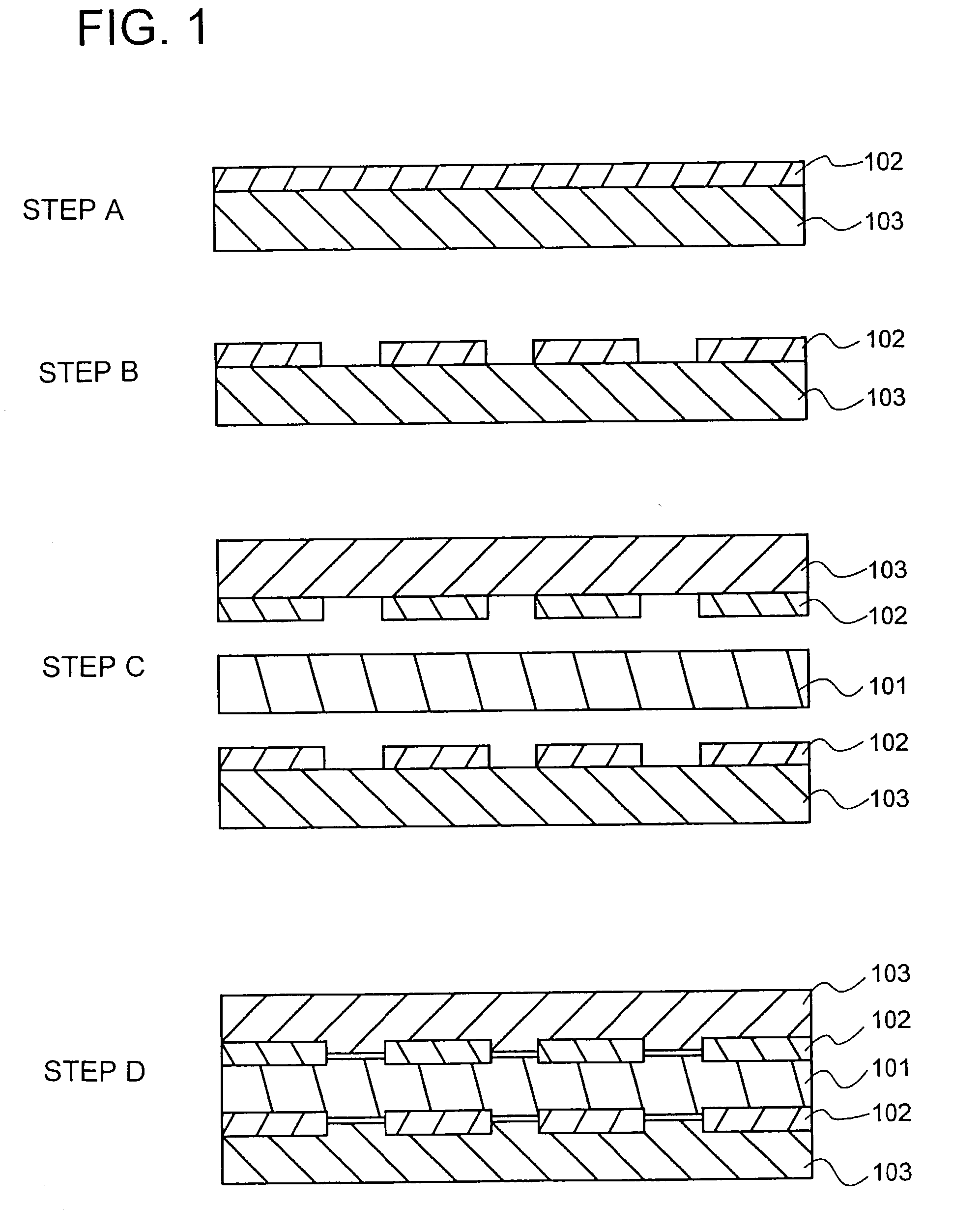
[0193] Next, a predetermined pattern was formed on the copper foil side of the prepreg by means of photolithography by immersing the prepr...

example 2

[0198] The sheet including no glass sheet produced in Example 1 was used to produce a multilayer substrate.

[0199] The transfer film used was a thermal release sheet (Intelimer Warm-off Type manufactured by Nitta K.K. which is a polyester supporting layer having a thickness of 100 .mu.m having thereon an adhesive layer of about 25 to 30 .mu.m thick), and to this transfer film was adhered a copper foil having a thickness of 18 .mu.m. The adhesive strength of the thermal release sheet was 1.5 N / 25 mm, and attachment was conducted at a pressure of 1 kg / mm.sup.2.

[0200] Next, a predetermined pattern was formed on the surface of the copper foil-clad surface by means of photolithography by immersing in an etching solution containing ferric chloride (35% solution, temperature 40.degree. C.) for about 10 to 15 minutes. Since the step of etching was conducted by means of a photolithographic technique, a fine pattern in the order of about 30 to 36 .mu.m could be formed clearly.

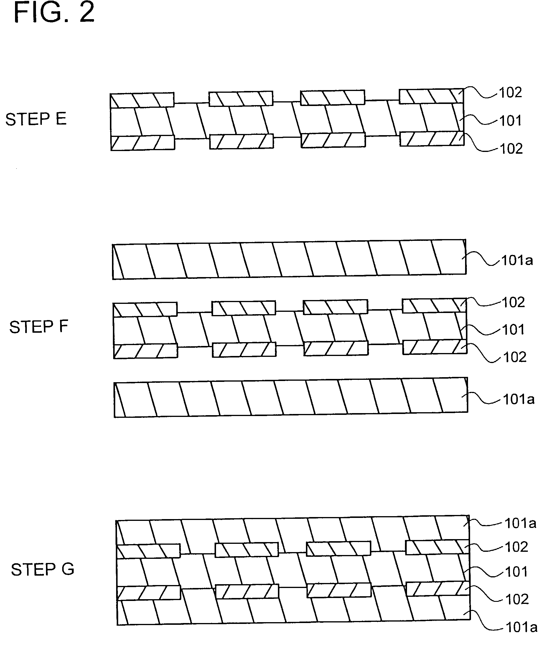
[0201] Next, two ...

example 3

[0203] FIGS. 3 and 4 illustrate an inductor. FIG. 3 is a see-through perspective view and FIG. 4 is a cross-sectional view.

[0204] In FIGS. 3 and 4, the inductor 10 includes constituent layers (prepregs or substrates) 10a to 10e of the resin materials of the invention, inner conductors (coil patterns) 13 formed on the constituent layers 10b to 10e, and via holes 14 for providing electrical connection to the inner conductors 13. Via holes 14 can be formed by drilling, laser machining, etching or the like. The ends of each coil formed are connected to through-vias 12 formed along end surfaces of the inductor 10 and land patterns 11 formed slightly above or below the through-vias 12. Through-via 12 has a half-cut structure by dicing or V-cutting. This is because when a plurality of devices are formed in a collective substrate which is eventually cut into discrete pieces along lines at the centers of through-vias 12.

[0205] At least one of the constituent layers 10a to 10e of the inductor...


PUM

PropertyMeasurementUnit
Pressureaaaaaaaaaa
Angleaaaaaaaaaa
Angleaaaaaaaaaa

Abstract

This invention has an object of providing a method for producing a multilayer substrate or an electronic part wherein decrease in the thickness has been enabled without causing the problem of insufficient strength or the like in the handling, as well as the electronic part. Such object has been attained by a method for producing a multilayer substrate or an electronic part comprising the steps of adhering a conductor layer to a transfer film, patterning the conductor layer to form a predetermined pattern, placing the transfer film overlaid with the patterned conductor layer on a prepreg so that the side of the conductor layer faces the prepreg, and then adhering the transfer film to the prepreg by applying heat and pressure and peeling the transfer film to produce the prepreg having the conductor layer formed thereon; and the multilayer electronic part produced by such method.

Description

CROSS-REFERENCES TO RELATED APPLICATIONS[0001] This application is a continuation of International PCT Application No. PCT / JP01 / 11499 filed on Dec. 27, 2001 which claims priority to Japanese patent application Nos. JPAP 2000-401493, filed on Dec. 28, 2000 and JPAP 2001-028854, filed on Feb. 5, 2001 in the Japanese Patent Office.BACKGROUND OF THE INVENTION[0002] 1. Field of the Invention[0003] This invention relates to a method for producing a multilayer substrate or an electronic part wherein a prepreg or a substrate is used, and also, to an electronic part produced by such method. More specifically, this invention relates to a method for producing a multilayer substrate or an electronic part as well as an electronic part wherein decrease in the layer thickness has been enabled.[0004] 2. Description of the Related Art[0005] In the field of electronic equipment for communication, commercial and industrial applications, the current mounting technology seeks further miniaturization and...

Claims


Application Information

Patent Timeline
IPC IPC(8): H01F17/00H01F41/04H01G4/30H05K1/16H05K3/20
CPCH01F17/0006Y10T29/49155H01F41/041H01G4/308H05K1/0373H05K1/16H05K1/162H05K1/165H05K3/0052H05K3/06H05K3/20H05K3/403H05K3/429H05K3/4652H05K2201/0209H05K2201/086Y10T29/49124H01F17/0013
Inventor TAKAYA, MINORUENDO, TOSHIKAZUSASAKI, MASAMI
Owner TDK CORPARATION
Why Eureka
Try Eureka