Process for producing optical element, optical element, optical films using optical element, and illuminator and liquid crystal display each using optical element or optical films
a technology of optical elements and optical films, applied in the direction of polarising elements, thin material processing, instruments, etc., can solve the problems of poor thickness precision and in-plane unevenness in optical properties, insufficient brightness improvement, and decrease in front-view hue/slant-view hue characteristics, etc., to achieve wide wavelength range, high efficiency, and high suitability
- Summary
- Abstract
- Description
- Claims
- Application Information
AI Technical Summary
Benefits of technology
Problems solved by technology
Method used
Image
Examples
production example 2
[0041] Preparation of Mixed Solution
[0042] A monofunctional, acrylic, nematic liquid crystal monomer showing liquid crystal properties in the temperature range of from 80 to 210.degree. C. was mixed with a bifunctional acrylic chiral reagent in a ratio of 95:5 by weight. This mixture was dissolved in a solvent (methyl ethyl ketone) so as to achieve a concentration of about 33% by weight. A polymerization initiator was added thereto in an amount of 5% by weight based on the weight of the sum of the monomer and the chiral reagent. Thus, a mixed solution A was prepared.
production example 3
[0043] Preparation of Mixed Solution
[0044] A bifunctional, acrylic, nematic liquid crystal monomer showing liquid crystal properties in the temperature range of from 80 to 210.degree. C. was mixed with a bifunctional acrylic chiral reagent in a ratio of 95:5 by weight. This mixture was dissolved in a solvent (methyl ethyl ketone) so as to acheive a concentration of about 33% by weight. A polymerization initiator was added thereto in an amount of 5% by weight based on the weight of the sum of the monomer and the chiral reagent. Thus, a mixed solution B was prepared.
example 1
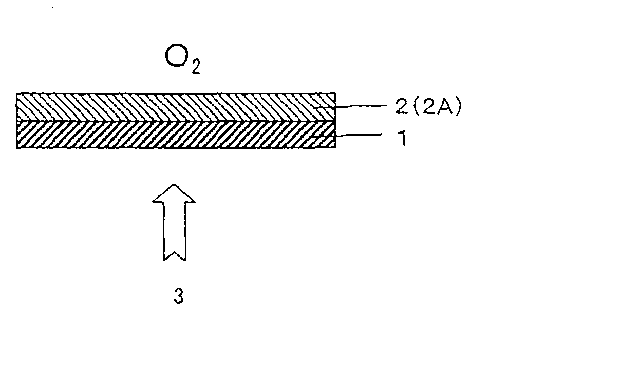
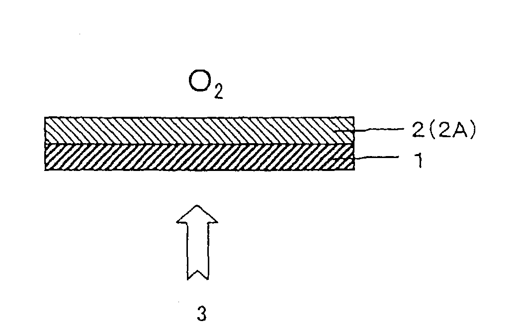
[0049] The mixed solution B was applied to the oriented substrate (orientation treatment side) and the solvent was removed by volatilization. Thereafter, the coated substrate was heated to 120.degree. C. to align the liquid crystal and then irradiated, from the oriented substrate side, with 100 mW / cm.sup.2 ultraviolet rays at 60.degree. C. in air for 2 seconds using a metal halide lamp. Thus, a thin film was obtained. This film had a thickness of 5 .mu.m.
PUM
 Abstract
Description
Claims
Application Information

