Method of manufacturing micro-lens array, electrolyte and manufacturing apparatus used therefor

a manufacturing method and technology of micro-lens array, applied in the field of manufacturing micro-lens array, electrolyte and manufacturing apparatus used therefor, can solve the problems of difficult curvature control of lens, long etching time of etching method, and difficult control of lens curvatur

Inactive Publication Date: 2003-07-31
FUJIFILM BUSINESS INNOVATION CORP
View PDF0 Cites 30 Cited by
  • Summary
  • Abstract
  • Description
  • Claims
  • Application Information

AI Technical Summary

Problems solved by technology

In the photolithographic process, any micro-lens array at high resolution power can be formed but the control for the curvature of lens is difficult.
The dry etching method requires a long etching time and involves difficulty for the curvature control of lens.
The method of providing a previously formed mold involves a problem in view of the restriction for the micro miniaturization of the mold.
Further, all the techniques mentioned above require high cost, and a technique for forming a micro-lens, which is simple and convenient and has a high degree of freedom, has not yet been available at present.
Further, as a low-cost method, there is a method of burying micro beads in a binder resin but it involves a problem that a uniform arrangement of micro beads is difficult.

Method used


Image

  • Method of manufacturing micro-lens array, electrolyte and manufacturing apparatus used therefor
  • Method of manufacturing micro-lens array, electrolyte and manufacturing apparatus used therefor
  • Method of manufacturing micro-lens array, electrolyte and manufacturing apparatus used therefor

Examples


example 1

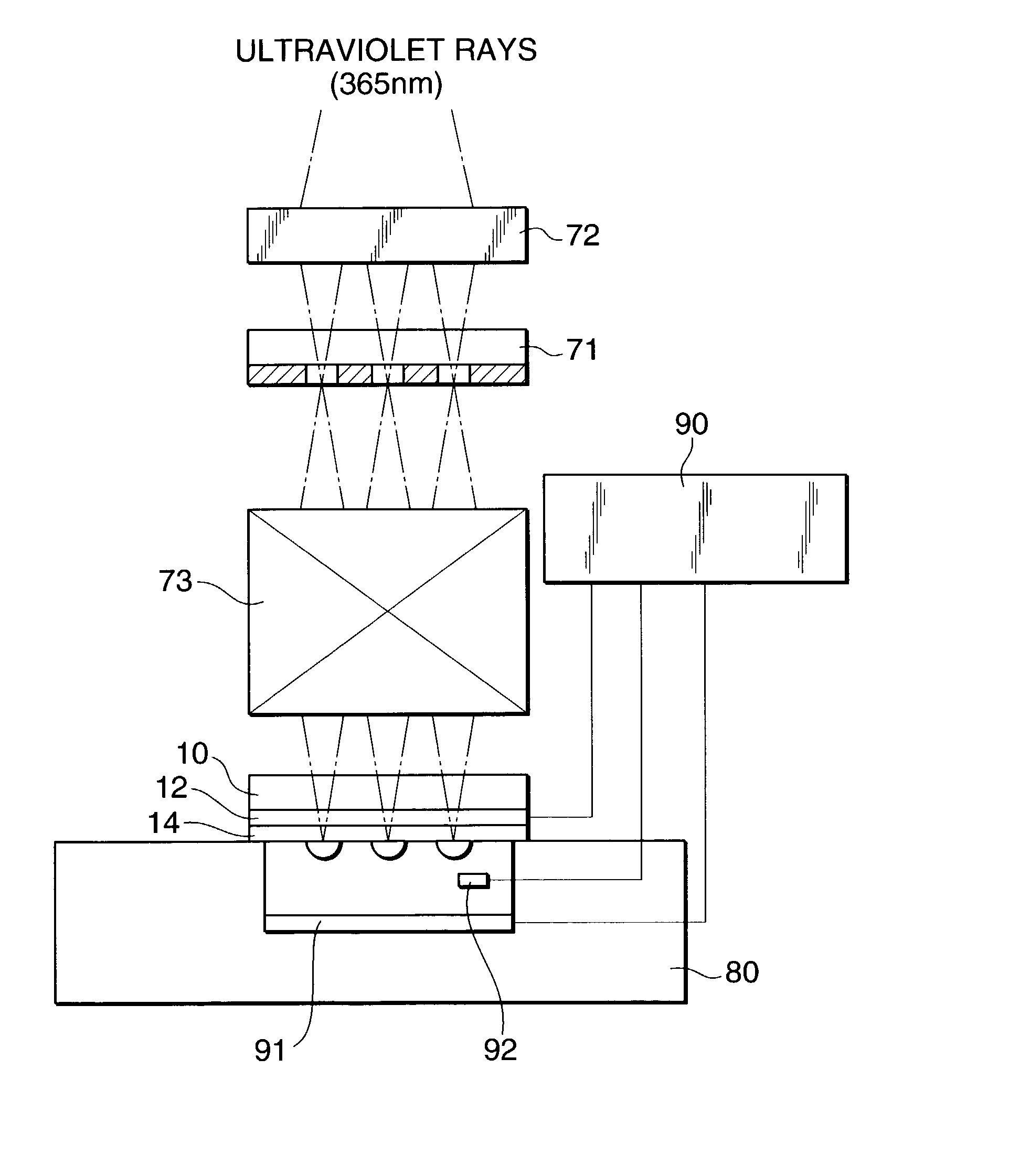
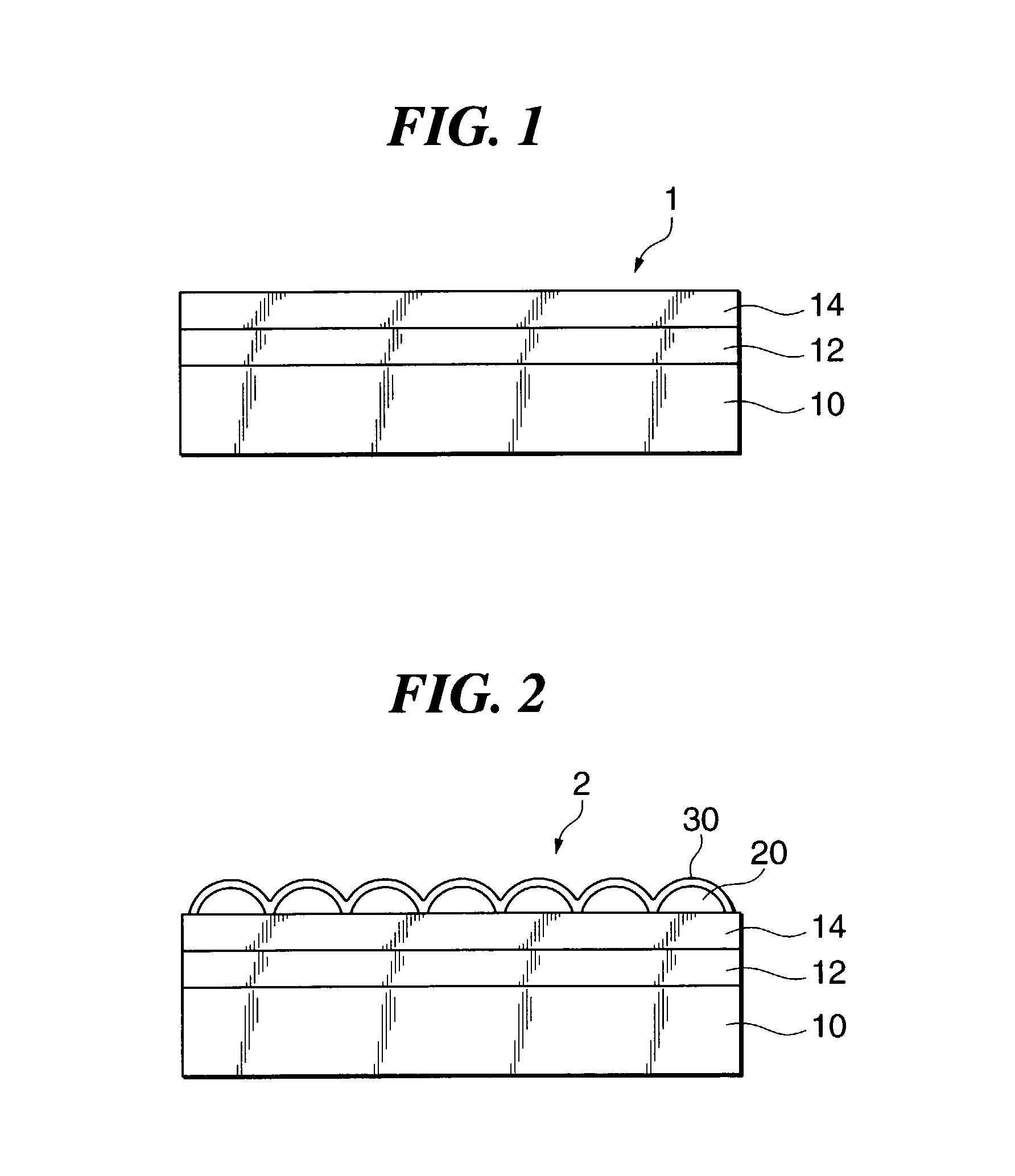
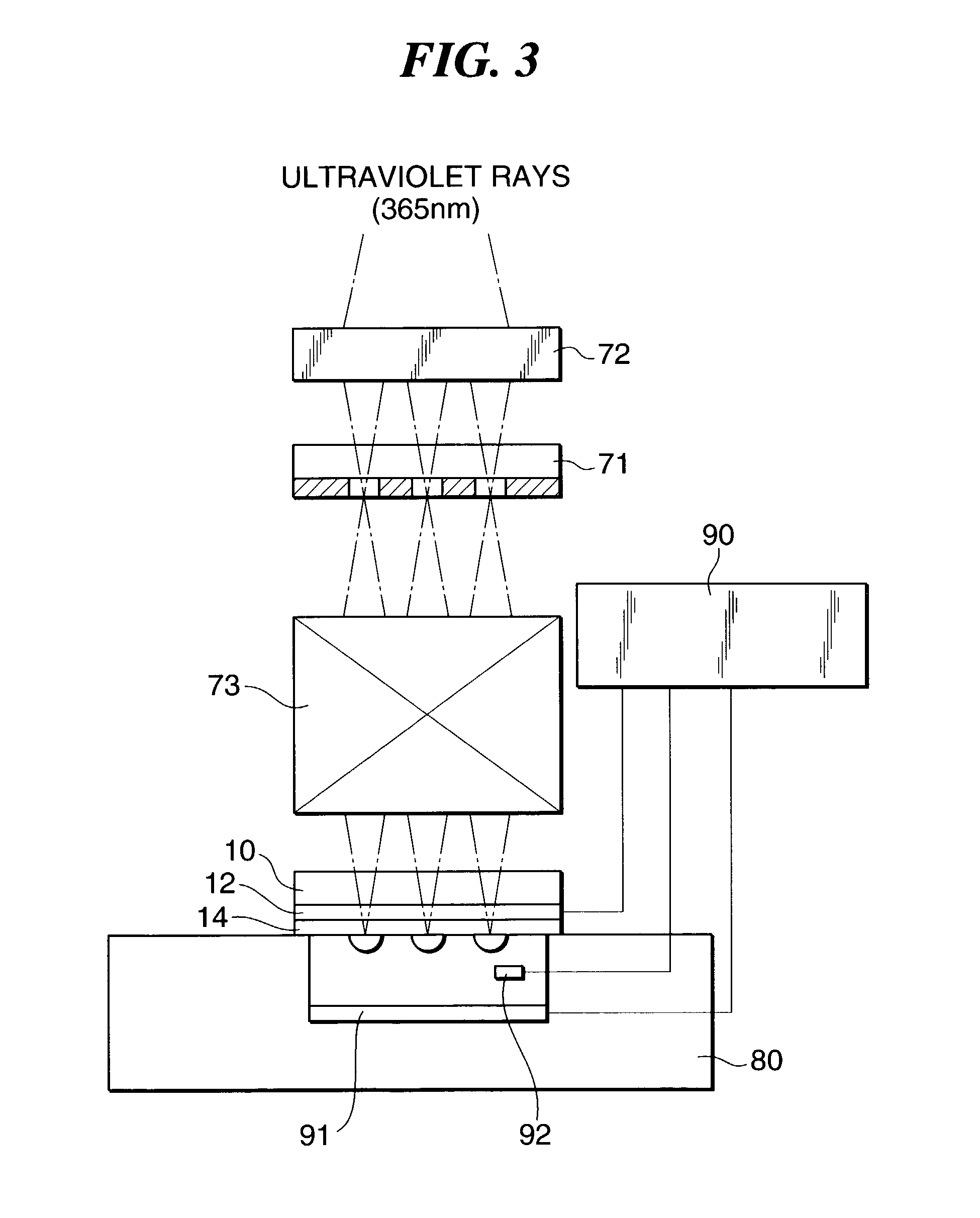
[0100] 75 nm of an ITO film and 110 nm of an anatase type thin titanium oxide film were formed by an RF sputtering method on an alkali-free glass substrate (7059 glass) of 0.4 mm in thickness to prepare a micro-lens array preparing substrate.

[0101] Then, an electrolyte including an aqueous liquid dispersion containing transparent fine particles (solid content: 10 mass %) was prepared by dispersing rutile type fine titanium oxide particles (grain size: 10 nm, refractive index: 2.7), styrene-acrylic acid copolymer (molecular weight: 13,000, molar ratio for hydrophobic group / (hydrophilic group+hydrophobic group): 0.65, acid value: 150) at a 1:5 volumic ratio, adding 5 mass % of ethylene glycol and further, using tetramethyl ammonium hydroxide and ammonium chloride to control pH to 7.8 and conductivity to 6 mS / cm.

[0102] A three-electrode type customary electrodeposition apparatus in electrochemistry shown in FIG. 3 was used and a TiO.sub.2 thin film as a micro-lens array preparing subst...

example 2

[0110] Electrodeposition was conducted by use of the same micro-lens array preparing substrate, photo-mask, electrolyte and electrodeposition conditions as those in Example 1 except for using a micro-lens array manufacturing apparatus shown in FIG. 4. A mercury xenon lamp (manufactured by Yamashita Denso Corporation, light intensity: 50 mW / cm.sup.2, wavelength: 365 nm) was used as the exposure device and the photo-mask was made in intimate contact with the glass substrate of the micro-lens array preparing substrate.

[0111] Further, heat treatment was applied at 150.degree. C. in the same manner as in Example 1 and a 96-nm SiO.sub.2 film was formed to obtain a micro-lens array.

[0112] The same micro-lens array as in Example 1 was obtained.

example 3

[0113] Electrodeposition was conducted by use of the same micro-lens array preparing substrate, photo-mask, electrolyte and electrodeposition conditions as those in Example 1 except for using a laser beam exposure device instead of using the projection type exposure device used in Example 1. A laser beam exposure device using an He--Cd laser, operationally associated with a Galvano scanner and an AO modulator and capable of turning on and off the laser beam at a predetermined position was used. The laser beam was formed as a Gaussian beam in which the intensity of light was increased toward the beam center and decreased toward the periphery. Exposure was conducted while scanning by the exposure apparatus.

[0114] Further, heat treatment was applied at 150.degree. C. in the same manner as in Example 1 and a 96-nm SiO.sub.2 film was formed to obtain a micro-lens array.

[0115] The same micro-lens array as in Example 1 was obtained.

[0116] The method of manufacturing the micro-lens array ac...


PUM

PropertyMeasurementUnit
diameteraaaaaaaaaa
heat resistanceaaaaaaaaaa

Abstract

A method includes the steps of disposing a substrate having a conductive thin film and a photo-semiconductor thin film in this order on an insulative base in an aqueous electrolyte material that solubility is lowered by a change of pH, irradiating with light a selected region of the photo-semiconductor thin film and precipitating the material to the selected region of the photo-semiconductor thin film to form a micro-lens array layer.

Description

[0001] 1. Field of the Invention[0002] This invention relates to a method of manufacturing a micro-lens array callable of condensing light at a high efficiency, as well as an electrolyte used therefore and an apparatus for manufacturing the micro-lens array.[0003] 2. Description of the Related Art[0004] A method of manufacturing a micro-lens array includes a photo-lithographic process, an etching process such as dry etching, a method of doping a high refractive index material by thermal diffusion or a method of casting a plastic material into a previously formed mold thereby forming a micro-lens array. In the photolithographic process, any micro-lens array at high resolution power can be formed but the control for the curvature of lens is difficult. The dry etching method requires a long etching time and involves difficulty for the curvature control of lens. The method of doping the high refractive index material by thermal diffusion has an advantage of a material being a flat plate...

Claims


Application Information

Patent Timeline
Patent Type & Authority Applications(United States)
IPC IPC(8): B29C33/38B29C39/02B29D11/00C25D5/02C25D9/00C25D9/02G02B1/11G02B1/113G02B3/00
CPCC25D5/024C25D9/00C25D7/12G02B3/0012C25D9/02
Inventor OHTSU, SHIGEMISHIMIZU, KEISHIYATSUDA, KAZUTOSHIAKUTSU, EIICHI
Owner FUJIFILM BUSINESS INNOVATION CORP
Why Eureka
Try Eureka