

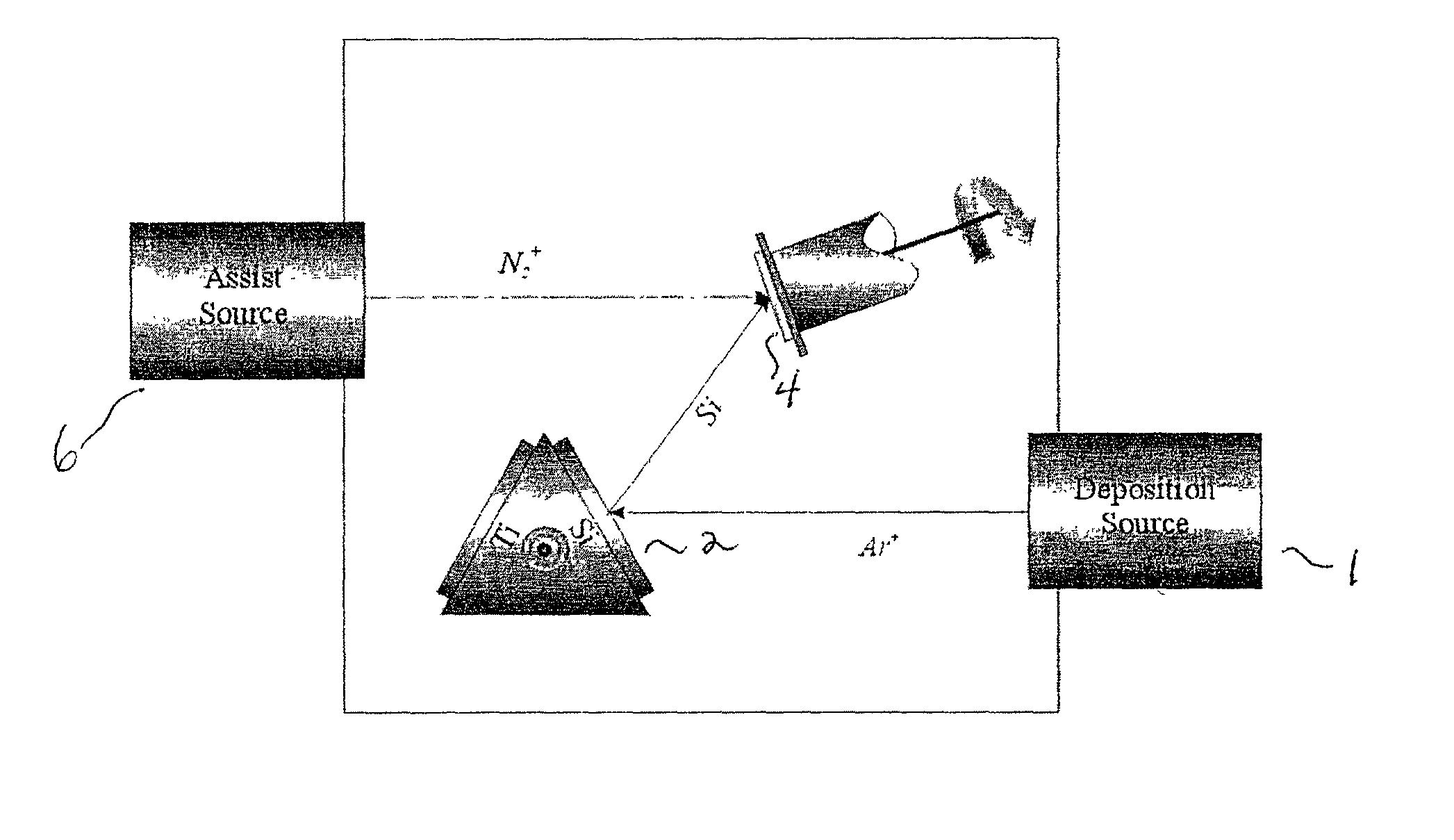
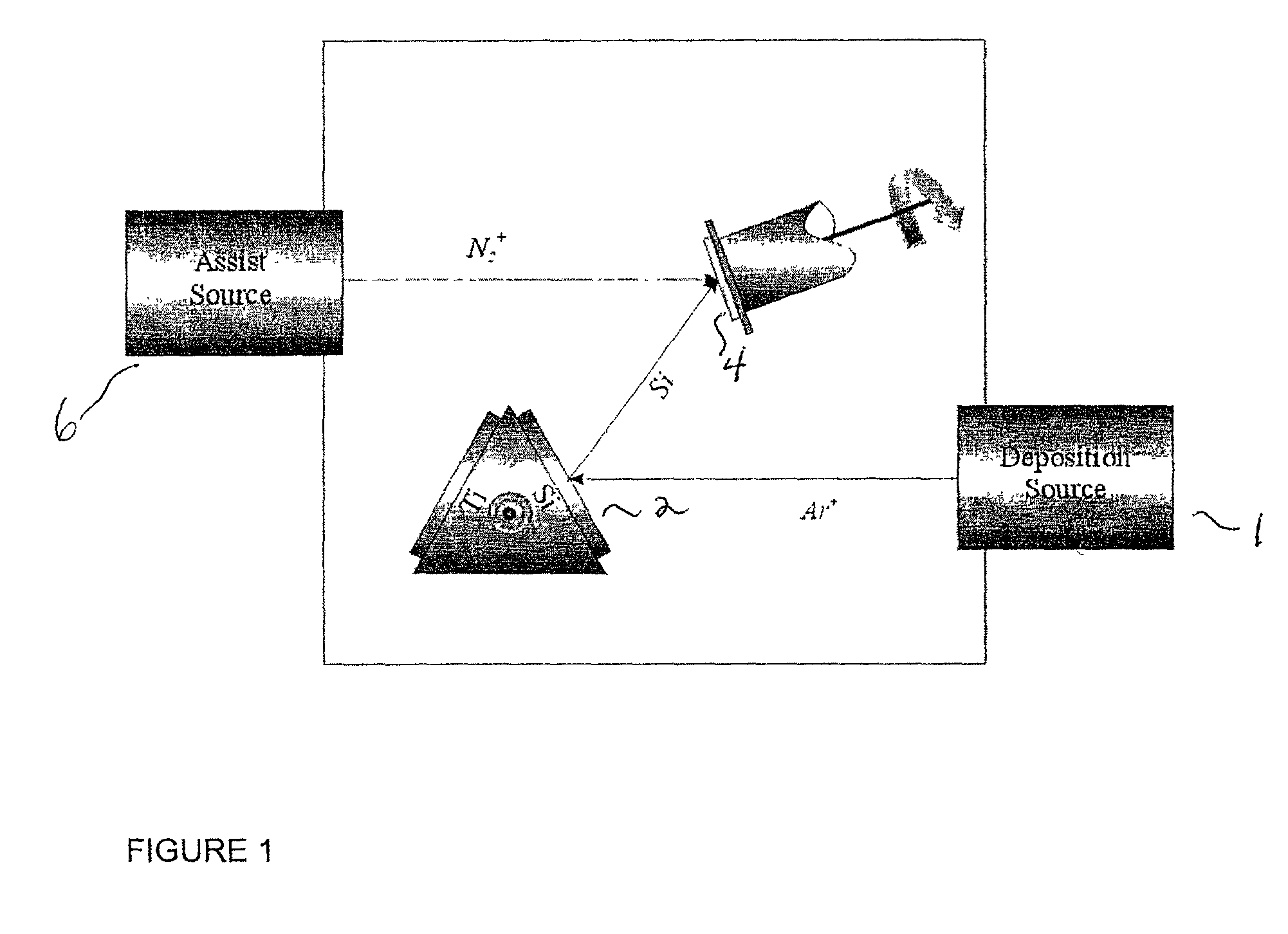
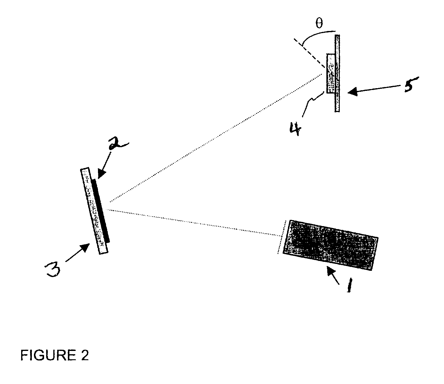
Ion-beam deposition process for manufacture of binary photomask blanks
a technology of ion beam and photomask, which is applied in the direction of photomechanical treatment originals, instruments, vacuum evaporation coating, etc., can solve the problems of inability to achieve the minimum feature size of the wafer with a particular wavelength of ligh
- Summary
- Abstract
- Description
- Claims
- Application Information
AI Technical Summary
Problems solved by technology
Method used
Image

Examples
Embodiment Construction
Opaque "Chrome" Mask
[0044] CrC.sub.xO.sub.yN.sub.z films, commonly used as a mask in traditional photolithography, were made by dual ion beam deposition in a commercial tool (Veeco IBD-210) from a Cr target. During deposition from the Cr target, the chemistry of the growing film was tailored by bombarding it with low energy ions derived from a gas mixture of CO.sub.2 and N.sub.2 diluted with Ar. The deposition ion beam source was operated at a voltage of 1500 V at a beam current of 200 mA, using 4 sccm of Xe. The assist source with 18 sccm of N.sub.2, 4 sccm of CO.sub.2 and 2 sccm of Ar was operated at 100 V and a current of 150 mA. The substrate was a five-inch square quartz plate, 0.09 inch thick. The deposition was continued for 15 min and yielded a film about 238 nm thick with an optical density measured at 248 nm of greater than 3, adequate for binary mask application in photolithography. A depth profile of the chemical composition of the film obtained by X-ray photoelectron sp...
PUM
| Property | Measurement | Unit |
|---|---|---|
| Nanoscale particle size | aaaaa | aaaaa |
| Wavelength | aaaaa | aaaaa |
| Wavelength | aaaaa | aaaaa |
Abstract
Description
Claims
Application Information