Printed circuit board,its manufacturing method and csp manufacturing method

a manufacturing method and printed circuit board technology, applied in the field of printed circuit boards, can solve problems such as achieve the effects of reducing the degree of handling freedom, and reducing the cost of manufacturing

Inactive Publication Date: 2004-05-27
MITSUI MINING & SMELTING CO LTD
View PDF8 Cites 14 Cited by
  • Summary
  • Abstract
  • Description
  • Claims
  • Application Information

AI Technical Summary

Benefits of technology

0054] In the fabrication method of the CSP of the present invention, the through-hole formation and the filling of the through-hole with the conductive material which are heretofore separately conducted can be conducted in a single operation during the fabrication of the respective unit print circuit boards. Accordingly, the respective unit print circuit boards can be fabricated easily or in a shorter period of time so that the CSP can be efficiently fabricated by the length of time obtained by mu

Problems solved by technology

Accordingly, a series of steps including the formation of the wired patterns on the print circuit board

Method used


Image

  • Printed circuit board,its manufacturing method and csp manufacturing method
  • Printed circuit board,its manufacturing method and csp manufacturing method
  • Printed circuit board,its manufacturing method and csp manufacturing method

Examples


example 1

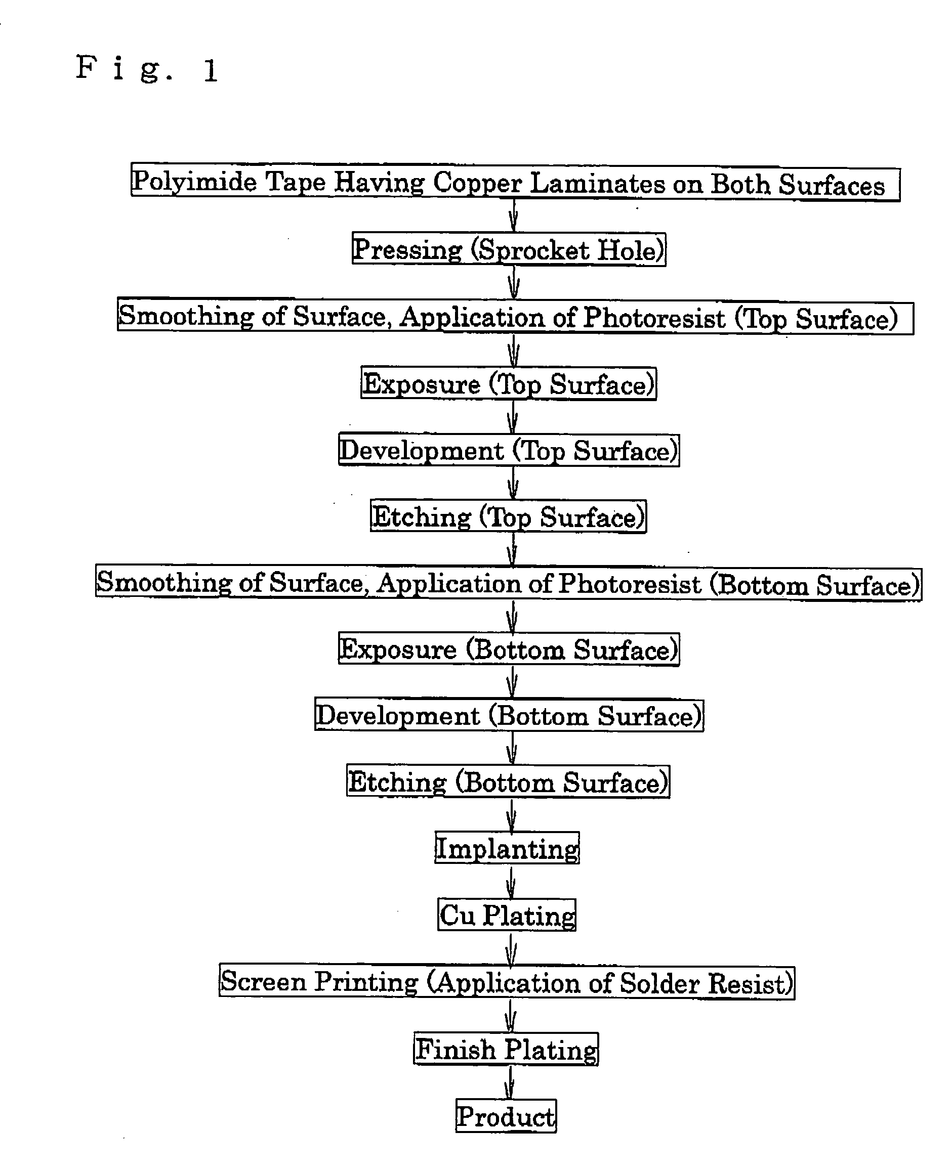
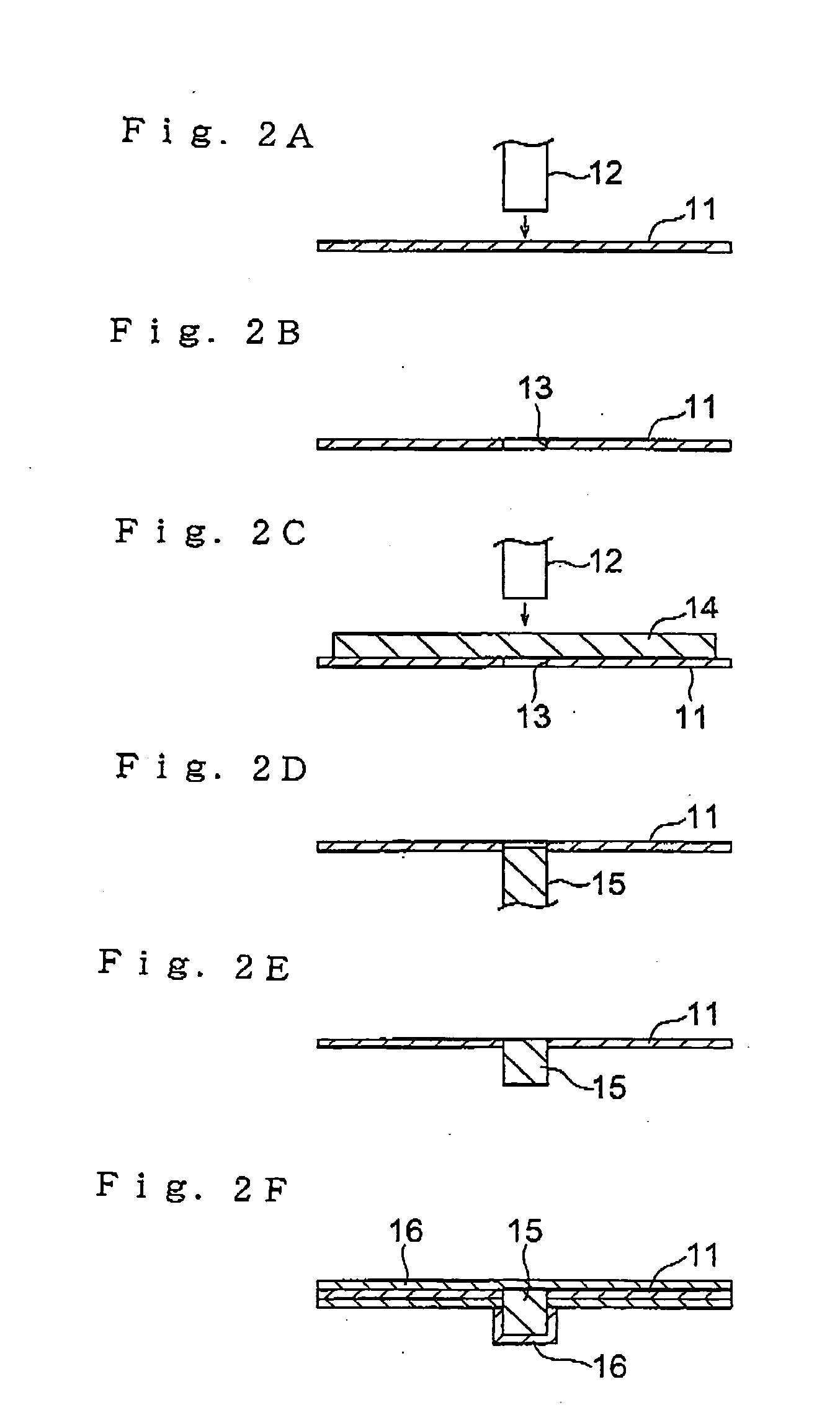
[0082] A conductor wired layer having bump was fabricated with procedures shown in FIG. 2.

[0083] A plurality of openings having a diameter of about 100 .mu.m were perforated through a copper foil (conductor wired layer) having a thickness of 18 .mu.m by using a punch having a diameter of about 100 .mu.m. On the copper foil was superposed a copper foil (conductor layer for forming bump) having a thickness of about 130 .mu.m. The copper foil (conductor layer for forming bump) was punched at the positions corresponding to the respective openings by using the above punch such that the copper foil is entered into the openings to be projected from the bottom edge of the openings and to form bumps, thereby obtaining a conductor wired layer with bumps. Lengths of the downward projection of the bumps were not uniform in the range of 100 to 130 .mu.m.

[0084] The conductor wired layer was caulked by using an ordinary caulking machine such that the lengths of the downward projection of the bumps...

example 2

[0088] A polyimide film (trade name: Espanex, available from Nippon Steel Chemical Co., Ltd.) substrate with a width of 35 mm and a thickness of 50 .mu.m having a copper foil with a thickness of 18 .mu.m laminated on its one surface was used. After a desired wired pattern was formed on the surface of the polyimide film substrate by etching the copper foil, annealed oxygen free high conductivity copper having a plate-like shape was positioned above the substrate.

[0089] After punches having a diameter of 80 .mu.m the same as a scheduled diameter of bumps made of the oxygen free high conductivity copper were placed at the positions corresponding to the bump formation on the substrate, the punches were strongly pressed downward for hollowing out the plate-like oxygen free high conductivity copper in the column shape followed by a similar hollow-out of the substrate to form though-holes. The through-holes were immediately filled with the hollowed oxygen free high conductivity copper to p...


PUM

PropertyMeasurementUnit
Electrical conductivityaaaaaaaaaa
Electrical conductoraaaaaaaaaa
Heightaaaaaaaaaa

Abstract

A printed circuit board comprising an insulating substrate, a through-hole formed in the insulating substrate, an implant material filling the through-hole, and a wiring pattern formed on both faces of the insulating substrate and electrically connected with the implant material, characterized in that one face of a conductor wiring layer wherein a bump penetrates from one face to the other face and protrudes is adhered to the insulating substrate so as to be electrically connected to the implant material. This bump conductor wiring layer of this printed circuit board has a large degree of freedom in forming a wiring pattern, through-hole, and bump and is unlike conventional handled separately from the insulating substrate. Therefore, the effect arises that this circuit board is the target of commercial trading by itself.

Description

[0001] The present invention relates to a print circuit board, a method for fabricating the same and a method for fabricating a chip size package (CSP) formed by stacking the print circuit boards ("CSP formed by stacking the print circuit boards" will be hereinafter referred to simply as "CSP"), and more specifically relates to the print circuit board fabricated by integrating wiring patterns formed separately from a dielectric substrate with the said dielectric substrate, the method for fabricating the same, and the method for fabricating the CSP with a higher productivity.[0002] Various circuit boards are used having conductor layers (wiring patterns) on their top and bottom surfaces. Concrete examples thereof includes a multi-layered wiring board using a rigid substrate made of glass epoxy in addition to a TAB (Tape Automated Bonding) tape using flexible polyimide resin as a substrate, CSP (Chip Size Package), BGA (Ball Grid Array) and FPC (Flexible Printed Circuit).[0003] The pr...

Claims


Application Information

Patent Timeline
IPC IPC(8): H01L21/48H01L21/98H01L23/498H01L25/065H01L25/10H05K3/00H05K3/40H05K3/46
CPCH01L21/486Y10T29/49126H01L23/49827H01L25/0657H01L25/50H01L2224/16H01L2225/06517H01L2225/0652H01L2225/06541H01L2225/06572H01L2225/06586H01L2924/01078H01L2924/01079H01L2924/15311H05K3/005H05K3/4046H05K3/4614H05K3/4617H05K2201/10416H05K2203/033H01L2225/1023H01L2225/1058Y10T29/49128Y10T29/49165H01L23/49816H01L2924/00014H01L2224/16225H01L2224/0401
Inventor ICHIRYU, AKIRAHAYASHI, KATSUHIKOKARAOKA, TATSUOKAWAMURA, HIROKAZUISHII, MASAHITO
Owner MITSUI MINING & SMELTING CO LTD
Why Eureka
Try Eureka