Ion-beam deposition process for manufacturing attenuated phase shift photomask blanks

a phase shift photomask and phase shift technology, which is applied in the direction of photomechanical treatment originals, instruments, electrographic processes, etc., can solve the problems of etching or removal of film, inability to accurately control the process of sputtering plasma, and limited resolution for imaging the minimum feature size on the wafer with a particular wavelength of ligh

Inactive Publication Date: 2004-06-17
EI DU PONT DE NEMOURS & CO
View PDF12 Cites 12 Cited by
  • Summary
  • Abstract
  • Description
  • Claims
  • Application Information

AI Technical Summary

Problems solved by technology

However, as the feature size decreases, resolution for imaging the minimum feature size on the wafer with a particular wavelength of light is limited by the diffraction of light.
Furthermore, the IBD process has the ability to independently control the deposition flux and the reactive gas ion flux (current) and energy, which are coupled and not independently controllable in planar magnetron sputtering.
While magnetron sputtering is extensively used in the electronics industry for reproducibly depositing all sorts of coatings, process control in sputtering plasmas is not accurate because the direction, energy, and flux of the ions incident on the growing film cannot be regulated.
For the "assist" ions, lower energy typically<500 eV is preferred, otherwise the ions may cause undesirable etching or removal of the film.
While it is possible to make films with complex chemical compounds, such as Si.sub.3N.sub.4, with ion beam deposition using a single ion source, the process is more restrictive than for dual ion beam deposition.

Method used


Image

  • Ion-beam deposition process for manufacturing attenuated phase shift photomask blanks
  • Ion-beam deposition process for manufacturing attenuated phase shift photomask blanks
  • Ion-beam deposition process for manufacturing attenuated phase shift photomask blanks

Examples


example 1

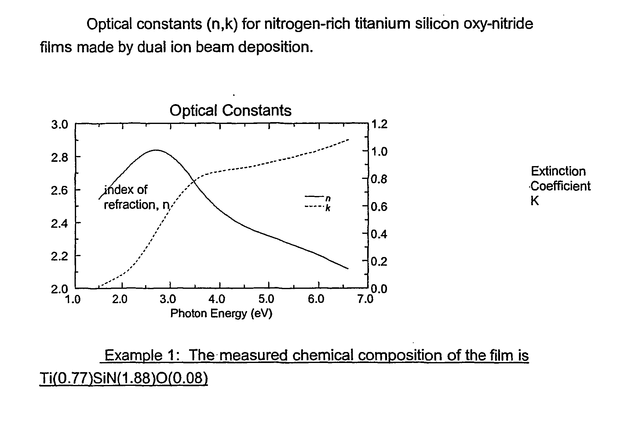
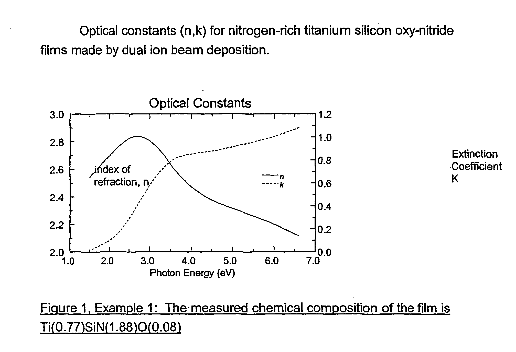
[0056] Titanium silicon nitride films were made by dual ion beam deposition in a commercial tool (Commonwealth Scientific) from a TiSi.sub.2 target. Deposition from TiSi.sub.2 was carried out with one ion beam deposition source operating at a voltage of 1200 V and a beam current of 25 mA, simultaneously nitriding the growing film with N.sub.2 ions from a second assist ion beam source, operating at 70 V. 20.6 sccm of Ar were used in the deposition source, while N.sub.2 at 7 sccm were used in the assist source. The substrates were Si and quartz. Deposition for 90 minutes produced a film 1175 A thick with chemical composition of Ti(0.77)SiN(1.88)O(0.08), as determined from X-ray photoelectron spectroscopy. FIG. 1 shows the spectral dependence of optical constants, determined by spectroscopic ellipsometry.

example 2

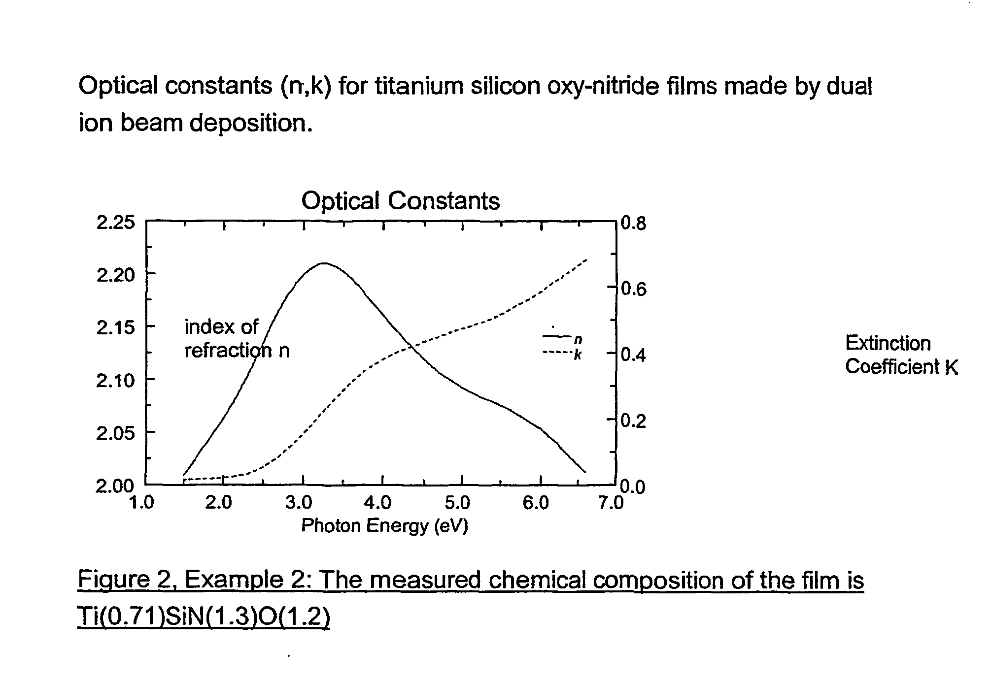
[0057] Titanium silicon oxy-nitride films were made by dual ion beam deposition in a commercial tool (Commonwealth Scientific) from a TiSi.sub.2 target. Deposition from TiSi.sub.2 was carried out with one ion beam deposition source operating at a voltage of 1200 V and a beam current of 25 mA, while the growing film was bombarded by ions from a 10% O.sub.2 / 90% N.sub.2 gas mixture from a second assist ion beam source, operating at 70 V. 16.6 sccm of Ar were used in the deposition source, while the flow rate of the O.sub.2 / N.sub.2 mixture was 2.9 sccm in the assist source. The substrates were Si and quartz. Deposition for 61 minutes produced a film 840 A thick with chemical composition of Ti(0.71)SiN(1.3)0(1.2), as determined from X-ray photoelectron spectroscopy. FIG. 2 shows the spectral dependence of optical constants, determined by spectroscopic ellipsometry.

example 3

[0058] Titanium silicon oxide films were made by dual ion beam deposition in a commercial tool (Commonwealth Scientific) from a TiSi.sub.2 target. Deposition from TiSi.sub.2 was carried out with one ion beam deposition source operating at a voltage of 1200 V and a beam current of 25 mA, simultaneously oxidizing the growing film with oxygen ions from a second assist ion beam source, operating at 70 V. 16.6 sccm of Ar were used in the deposition source, while the flow rate of the O.sub.2 was 3 sccm in the assist source. The substrates were Si and quartz. Deposition for 58 minutes produced a film 208 A thick with chemical composition of Ti(0.57)SiO(3.1), as determined from X-ray photoelectron spectroscopy. FIG. 3 shows the spectral dependence of optical constants, determined by spectroscopic ellipsometry.

[0059] These three examples follow the trend in optical properties for below 400 nm or greater than 3.1 eV in energy that increasing the oxide content in titanium silicon oxy-nitride f...


PUM

PropertyMeasurementUnit
lithographic wavelengthsaaaaaaaaaa
lithographic wavelengthaaaaaaaaaa

Abstract

An ion-beam deposition process for fabricating attenuating phase shift photomask blanks, capable of producing a phase shift of 180°, and which can provide tunable optical transmission at selected lithographic wavelengths<400 nm, comprising at least one layer of material of general formulae MzSiOxNy or MzAlOxNy, is described.

Description

[0001] This invention relates to manufacture of phase shift photomask blanks in photolithography, known in the art as the attenuating (embedded) type, using the ion-beam deposition technique. More specifically, this invention relates to photomask blanks to be used with short wavelength (i.e., <400 nanometer) light, which attenuate and change the phase of transmitted light by 180.degree. relative to the incident light, and which provide tunable optical transmission. Additionally, this invention relates to photomask blanks with single or multi-layered coating of the general formula MxSiOyNz or MxAlOyNz on the blanks.TECHNICAL BACKGROUND[0002] Microlithography is the process of transferring microscopic circuit patterns or images, usually through a photomask, on to a silicon wafer. In the production of integrated circuits for computer microprocessors and memory devices, the image of an electronic circuit is projected, usually with an electromagnetic wave source, through a mask or ste...

Claims


Application Information

Patent Timeline
Patent Type & Authority Applications(United States)
IPC IPC(8): C23C14/06C23C14/08C23C14/46G03F1/32G03F1/54G03F1/68
CPCC23C14/0641C23C14/0676C23C14/08G03F1/68G03F1/32G03F1/54C23C14/46
Inventor CARCIA, PETER FRANCIS
Owner EI DU PONT DE NEMOURS & CO
Why Eureka
Try Eureka